
Datasheet


November 2005
©2005 Fairchild Semiconductor Corporation
FDS4897C Rev C(W)
www.fairchildsemi.com
FDS4897C
Dual N & P-Channel PowerTrench
®
MOSFET
General Description
These dual N- and P-Channel enhancement mode
power field effect transistors are produced using
Fairchild Semiconductor’s advanced PowerTrench
process that has been especially tailored to minimize
on-state resistance and yet maintain superior switching
performance.
Application
• Inverter
• Power Supplies
Features
• Q1: N-Channel
6.2A, 40V R
DS(on)
= 29mΩ @ V
GS
= 10V
R
DS(on)
= 36mΩ @ V
GS
= 4.5V
• Q2: P-Channel
–4.4A, –40V R
DS(on)
= 46mΩ @ V
GS
= –10V
R
DS(on)
= 63mΩ @ V
GS
= –4.5V
• High power handling capability in a widely used
surface mount package
• RoHS compliant
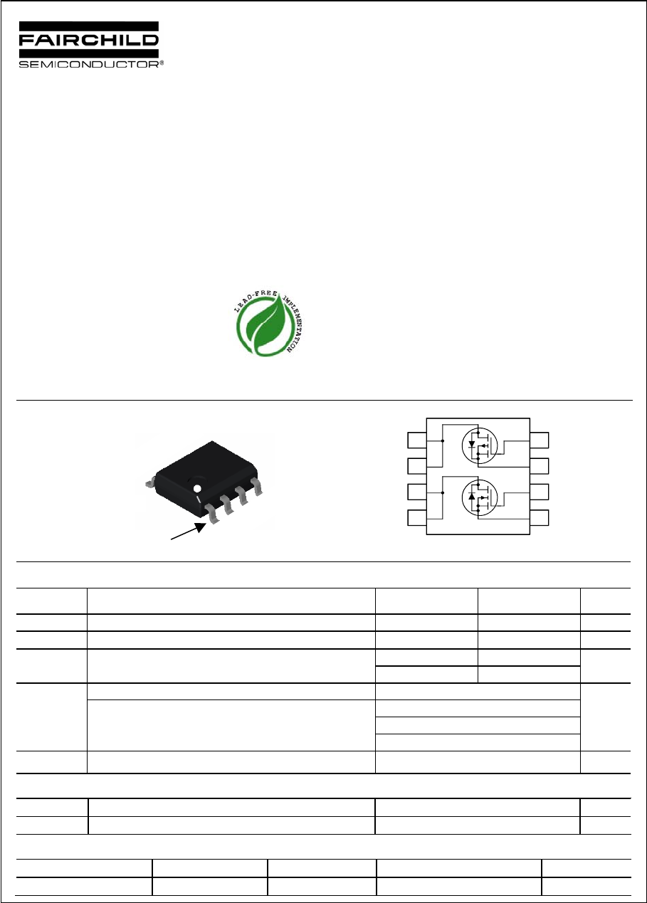
S
D
S
S
SO-8
D
D
D
G
D1
D1
D2
D2
S1
G1
S2
G2
Pin 1
SO-8
4
3
2
1
5
6
7
8
Q1
Q2
Absolute Maximum Ratings T
A
= 25°C unless otherwise noted
Symbol Parameter Q1 Q2 Units
V
DSS
Drain-Source Voltage 40 40 V
V
GSS
Gate-Source Voltage
±20 ±20
V
I
D
Drain Current - Continuous (Note 1a) 6.2 –4.4 A
- Pulsed 20 –20
P
D
Power Dissipation for Dual Operation 2 W
Power Dissipation for Single Operation (Note 1a) 1.6
(Note 1b)
1
(Note 1c)
0.9
T
J
, T
STG
Operating and Storage Junction Temperature Range –55 to +150
°C
Thermal Characteristics
R
θJA
Thermal Resistance, Junction-to-Ambient
(Note 1a) 78
°C/W
R
θJC
Thermal Resistance, Junction-to-Case
(Note 1) 40
°C/W
Package Marking and Ordering Information
Device Marking Device Reel Size Tape width Quantity
FDS4897C FDS4897C 13” 12mm 2500 units
FD
S
4
89
7
C
D
ua
l N
&
P-
C
h
a
nn
e
l P
o
w
e
rTr
e
n
c
h
®
M
OS
FET