
Datasheet


©2010 Fairchild Semiconductor Corporation 1 www.fairchildsemi.com
March 2010
FDS6930B Rev. A1
FDS6930B Dual N-Channel Logic Level PowerTrench
®
MOSFET
FDS6930B
Dual N-Channel Logic Level PowerTrench
®
MOSFET
Features
■ 5.5 A, 30 V. R
DS(ON)
= 38 m
Ω @ V
GS
= 10 V
R
DS(ON)
= 50 m
Ω @ V
GS
= 4.5 V
■ Fast switching speed
■ Low gate charge
■ High performance trench technology for extremely
low R
DS(ON)
■ High power and current handling capability
General Description
These N-Channel Logic Level MOSFETs are produced using
Fairchild Semiconductor’s advanced PowerTrench process that
has been especially tailored to minimize the on-state resistance
and yet maintain superior switching performance.
These devices are well suited for low voltage and battery pow-
ered applications where low in-line power loss and fast switch-
ing are required.
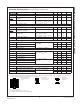
Absolute Maximum Ratings
T
A
= 25°C unless otherwise noted
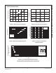
Package Marking and Ordering Information
Symbol Parameter Ratings Units
V
DSS
Drain-Source Voltage 30 V
V
GSS
Gate-Source Voltage
± 20 V
I
D
Drain Current – Continuous (Note 1a) 5.5 A
– Pulsed 20
P
D
Power Dissipation for Dual Operation (Note 1) 2 W
Power Dissipation for Single Operation (Note 1a) 1.6
(Note 1b) 1
(Note 1c) 0.9
T
J
, T
STG
Operating and Storage Junction Temperature Range –55 to 150
°C
Thermal Characteristics
R
θJA
Thermal Resistance, Junction-to-Ambient (Note 1a) 78
°C/W
R
θJC
Thermal Resistance, Junction-to-Case (Note 1) 40
°C/W
Device Marking Device Reel Size Tape width Quantity
FDS6930B FDS6930B 13" 12mm 2500 units
D1
D1
D2
D2
S1
G1
S2
G2
Pin 1
SO-8
45
36
27
18