
Datasheet


2 www.fairchildsemi.com
FDS6930B Rev. A1
FDS6930B Dual N-Channel Logic Level PowerTrench
®
MOSFET
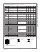
Electrical Characteristics T
A
= 25°C unless otherwise noted
Notes:
1. R
θJA
is the sum of the junction-to-case and case-to-ambient thermal resistance where the case thermal reference is defined as the solder mounting surface of the drain pins.
R
θJC
is guaranteed by design while R
θCA
is determined by the user's board design.
Scale 1 : 1 on letter size paper
2. Pulse Test: Pulse Width < 300
µs, Duty Cycle < 2.0%
3. Trr parameter will not be subjected to 100% production testing.
Symbol Parameter Test Conditions Min Typ Max Units
Off Characteristics
BV
DSS
Drain–Source Breakdown Voltage V
GS
= 0 V, I
D
= 250
µA30 V
∆BVDSS
∆T
J
Breakdown Voltage Temperature
Coefficient
I
D
= 250
µA, Referenced to 25
°C 26 mV/
°C
I
DSS
Zero Gate Voltage Drain Current V
DS
= 24 V, V
GS
= 0 V
V
DS
= 24 V, V
GS
= 0 V, T
J
= 55
°C
1
10
µA
I
GSS
Gate–Source Leakage V
GS
=
±20 V, V
DS
= 0 V
±100 nA
On Characteristics
(Note 2)
V
GS(th)
Gate Threshold Voltage V
DS
= V
GS
, I
D
= 250
µA 1 1.9 3 V
∆VGS(th)
∆T
J
Gate Threshold Voltage
Temperature Coefficient
I
D
= 250
µA, Referenced to 25
°C –4.6 mV/
°C
R
DS(on)
Static Drain–Source
On–Resistance
V
GS
= 10 V, I
D
= 5.5 A
V
GS
= 4.5 V, I
D
= 4.8 A
V
GS
= 10 V, I
D
= 5.5 A, T
J
= 125
°C
31
40
45
38
50
62
m
Ω
I
D(on)
On–State Drain Current V
GS
= 10 V, V
DS
= 5 V 20 A
g
FS
Forward Transconductance V
DS
= 5 V, I
D
= 5.5 A 19 S
Dynamic Characteristics
C
iss
Input Capacitance V
DS
= 15 V, V
GS
= 0 V,
f = 1.0 MHz
310 412 pF
C
oss
Output Capacitance 90 120 pF
C
rss
Reverse Transfer Capacitance 40 60 pF
R
G
Gate Resistance V
GS
= 15 mV, f = 1.0 MHz 1.9
Ω
Switching Characteristics
(Note 2)
t
d(on)
Turn–On Delay Time V
DD
= 15 V, I
D
= 1 A,
V
GS
= 10 V, R
GEN
= 6
Ω
612 ns
t
r
Turn–On Rise Time 612 ns
t
d(off)
Turn–Off Delay Time 16 28 ns
t
f
Turn–Off Fall Time 24 ns
Q
g
Total Gate Charge V
DS
= 15 V, I
D
= 5.5 A,
V
GS
= 5 V
2.7 3.8 nC
Q
gs
Gate–Source Charge 1.0 nC
Q
gd
Gate–Drain Charge 0.7 nC
Drain–Source Diode Characteristics and Maximum Ratings
I
S
Maximum Continuous Drain–Source Diode Forward Current 1.3 A
V
SD
Drain–Source Diode Forward Voltage V
GS
= 0 V, I
S
= 1.3 A (Note 2) 0.8 1.2 V
t
rr
Diode Reverse Recovery Time
(note3)
I
F
= 5.5 A, d
iF
/d
t
= 100 A/µs 16 32 nS
Q
rr
Diode Reverse Recovery Charge 6 nC
a) 78°C/W when mounted
on a 0.5 in
2
pad of 2 oz
copper
b) 125°C/W when
mounted on a 0.02 in
2
pad of 2 oz copper
c) 135°C/W when
mounted on a
minimum pad.