
Datasheet

July 2011
©2011 Fairchild Semiconductor Corporation
FDS86106 Rev. C2
www.fairchildsemi.com
1
FDS86106 N-Channel Power Trench
®
MOSFET
FDS86106
N-Channel Power Trench
®
MOSFET
100 V, 3.4 A, 105 mΩ
Features
Max r
DS(on)
= 105 mΩ at V
GS
= 10 V, I
D
= 3.4 A
Max r
DS(on)
= 171 mΩ at V
GS
= 6 V, I
D
= 2.7 A
High performance trench technology for extremely low r
DS(on)
High power and current handling capability in a widely used
surface mount package
100% UIL Tested
RoHS Compliant
General Description
This N-Channel MOSFET is produced using Fairchild
Semiconductor‘s advanced Power Trench
®
process that has
been optimized for
r
DS(on)
, switching performance and
ruggedness
.
Applications
Synchronous Rectifier
Primary Switch For Bridge Topology
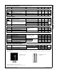
MOSFET Maximum Ratings T
A
= 25 °C unless otherwise noted
Thermal Characteristics
Package Marking and Ordering Information
Symbol Parameter Ratings Units
V
DS
Drain to Source Voltage 100 V
V
GS
Gate to Source Voltage ±20 V
I
D
Drain Current -Continuous 3.4
A
-Pulsed 15
E
AS
Single Pulse Avalanche Energy (Note 3) 13 mJ
P
D
Power Dissipation T
A
= 25 °C (Note 1a) 5.0
W
Power Dissipation T
A
= 25 °C (Note 1b) 2.5
T
J
, T
STG
Operating and Storage Junction Temperature Range -55 to +150 °C
R
θJC
Thermal Resistance, Junction to Case (Note 1) 2.5
°C/W
R
θJA
Thermal Resistance, Junction to Ambient (Note 1a) 50
Device Marking Device Package Reel Size Tape Width Quantity
FDS86106 FDS86106 SO-8 13 ’’ 12 mm 2500 units
SO-8
D
D
D
D
S
S
S
G
Pin 1
G
S
S
S
D
D
D
D
5
6
7
8
3
2
1
4