
Datasheet

©2004 Fairchild Semiconductor Corporation www.fairchildsemi.com
FOD2743A, FOD2743B, FOD2743C Rev. 1.0.1 2
FOD2743A, FOD2743B, FOD2743C — Optically Isolated Error Amplifier
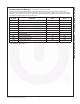
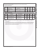
Pin Definitions
*The compensation network must be attached between pins 2 and 4.
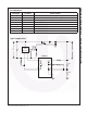
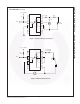
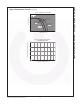
Typical Application
Pin Number Pin Name Pin Description
1 LED
Anode LED. This pin is the input to the light emitting diode.
2 COMP
Error Amplifier Compensation. This pin is the output of the error amplifier. *
3 GND
Ground
4FB
Voltage Feedback. This pin is the inverting input to the error amplifier
5NC
Not connected
6E
Phototransistor Emitter
7C
Phototransistor Collector
8NC
Not connected
V
O
V
1
R1
R2
7
6
1
2
4
3
PWM
Control
FAN4803
FOD2743