
Datasheet

©2004 Fairchild Semiconductor Corporation www.fairchildsemi.com
FOD2743A, FOD2743B, FOD2743C Rev. 1.0.1 3
FOD2743A, FOD2743B, FOD2743C — Optically Isolated Error Amplifier
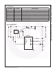
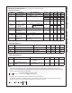
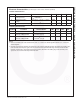
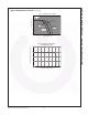
Absolute Maximum Ratings
(T
A
= 25°C unless otherwise specified)
Stresses exceeding the absolute maximum ratings may damage the device. The device may not function or be
operable above the recommended operating conditions and stressing the parts to these levels is not recommended.
In addition, extended exposure to stresses above the recommended operating conditions may affect device reliability.
The absolute maximum ratings are stress ratings only.
Note:
1. See derating graph, Figure 21.
Symbol Parameter Value Units
T
STG
Storage Temperature
-40 to +125 °C
T
OPR
Operating Temperature
-40 to +85 °C
T
SOL
Lead Solder Temperature
260 for 10 sec. °C
V
LED
Input Voltage
37 V
I
LED
Input DC Current
20 mA
V
CEO
Collector-Emitter Voltage
70 V
V
ECO
Emitter-Collector Voltage
7V
I
C
Collector Current
50 mA
PD1
Input Power Dissipation
145 mW
PD2
Transistor Power Dissipation
85 mW
PD3
Total Power Dissipation
(1)
145 mW