
Datasheet


©2009 Fairchild Semiconductor Corporation www.fairchildsemi.com
FODM611 Rev. 1.0.3 4
FODM611 — High Noise Immunity, 5V, 10Mbit/sec Logic Gate Output (Open Collector) Optocoupler
Electrical Characteristics
(Apply over all recommended conditions)
(T
A
= -40ºC to +85ºC, 4.5V
≤
V
CC
≤
5.5V), unless otherwise specified.
Typical value is measured at T
A
= 25ºC and V
CC
= 5.0V.
Switching Characteristics
(Apply over all recommended conditions)
(T
A
= -40ºC to +85ºC, 4.5V
≤
V
CC
≤
5.5V, I
F
= 7.5mA), unless otherwise specified.
Typical value is measured at T
A
= 25ºC and V
CC
= 5.0V
Notes
6. t
PSK
is equal to the magnitude of the worst case difference in t
PHL
and/or t
PLH
that will be seen between any two units
from the same manufacturing date code that are operated at same case temperature (±5°C), at same operating
conditions, with equal loads (R
L
= 350
Ω
and C
L
= 15pF), and with an input rise time less than 5ns.
7. Common mode transient immunity at output high is the maximum tolerable positive dVcm/dt on the leading edge of
the common mode impulse signal, Vcm, to assure that the output will remain high. Common mode transient immunity
at output low is the maximum tolerable negative dVcm/dt on the trailing edge of the common pulse signal, Vcm, to
assure that the output will remain low.
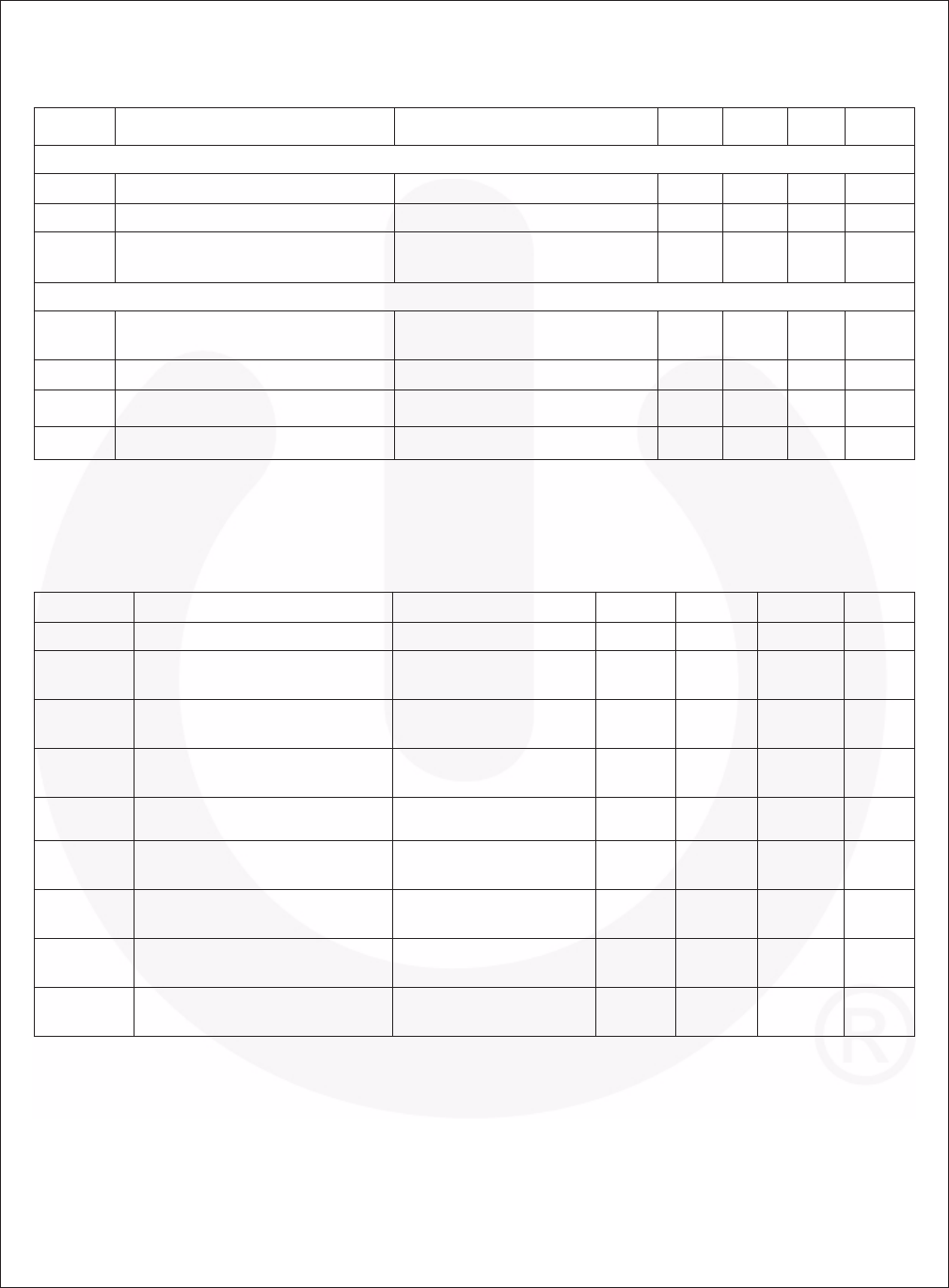
Symbol Parameter Test Conditions Min. Typ. Max. Units
INPUT CHARACTERISTICS
V
F
Forward Voltage I
F
= 10mA, Fig. 1 1.05 1.45 1.8 V
BV
R
Input Reverse Breakdown Voltage I
R
= 10µA 5.0 V
I
FHL
Threshold Input Current V
O
= 0.6V, I
OL
(sinking) = 13mA,
T
A
< 85ºC, Fig. 2
3.4 5.0 mA
OUTPUT CHARACTERISTICS
V
OL
Logic LOW Output Voltage I
F
= rated I
FHL
,
I
OL
(sinking) = 13mA, Fig. 3
0.4 0.6 V
I
OH
Logic HIGH Output Current I
F
= 250µA, V
O
= 5.0V, Fig. 4 2.1 30.0 µA
I
CCL
Logic LOW Output Supply Current I
F
= 10mA, V
CC
= 5.0V, Fig. 5, 7 7.5 10.0 mA
I
CCH
Logic HIGH Output Supply Current I
F
= 0mA, V
CC
= 5.0V, Fig. 6, 7 6.0 9.0 mA
Symbol Parameter Test Conditions Min. Typ. Max. Units
Date Rate R
L
= 350Ω 10 Mbps
t
PHL
Propagation Delay Time to Logic
Low Output
R
L
= 350Ω, C
L
= 15pF,
Fig. 8 and 11
43 100 ns
t
PLH
Propagation Delay Time to Logic
High Output
R
L
= 350Ω, C
L
= 15pF,
Fig. 8 and 11
50 100 ns
PWD Pulse Width Distortion,
| t
PHL
– t
PLH
|
R
L
= 350Ω, C
L
= 15pF,
Fig. 9
735ns
t
PSK
Propagation Delay Skew R
L
= 350Ω, C
L
= 15pF
(6)
40 ns
t
R
Output Rise Time, (10% to 90%) R
L
= 350Ω, C
L
= 15pF,
Fig. 10 and 11
20 ns
t
F
Output Fall Time, (90% to 10%) R
L
= 350Ω, C
L
= 15pF,
Fig. 10 and 11
10 ns
|CM
H
| Common Mode Transient
Immunity at Output High
V
I
= 5.0V, V
O
> 0.8 x V
CC
,
V
CM
= 1000V
(7)
, Fig. 12
20 40 kV/µs
|CM
L
| Common Mode Transient
Immunity at Output Low
V
I
= 0V, V
O
< 0.8V,
V
CM
= 1000V
(7)
, Fig. 12
20 40 kV/µs