
Datasheet


FQT1N60C N-Channel MOSFET
©2007 Fairchild Semiconductor Corporation
FQT1N60C Rev. C0
www.fairchildsemi.com1
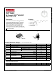
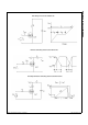
D
G
S
SOT-223
G
D
S
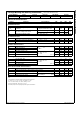
MOSFET Maximum Ratings T
C
= 25
o
C unless otherwise noted*
Thermal Characteristics
Symbol Parameter FQT1N60C
Unit
V
DSS
Drain to Source Voltage 600 V
V
GSS
Gate to Source Voltage ±30 V
I
D
D r a i n C u r r e n t
-Continuous (T
C
= 25
o
C) 0.2
A
-Continuous (T
C
= 100
o
C) 0.12
I
DM
D r a i n C u r r e n t - P u l s e d (Note 1) 0.8 A
E
AS
Single Pulsed Avalanche Energy (Note 2) 33 mJ
I
AR
Avalanche Current (Note 1) 0.2 A
E
AR
Repetitive Avalanche Energy (Note 1) 0.2 mJ
dv/dt Peak Diode Recovery dv/dt (Note 3) 4.5 V/ns
P
D
Power Dissipation
(T
C
= 25
o
C) 2.1 W
- Derate above 25
o
C0.02W/
o
C
T
J
, T
STG
Operating and Storage Temperature Range -55 to +150
o
C
T
L
Maximum Lead Temperature for Soldering Purpose,
1/8” from Case for 5 Seconds
300
o
C
Symbol Parameter
Min. Max.
Unit
R
θJA
Thermal Resistance, Junction to Ambient* - 60
o
C/W
* When mounted on the minimum pad size recommended (PCB Mount)
March 2013
FQT1N60C
Features
This N-Channel enhancement mode power MOSFET is
produced using Fairchild Semiconductor
®
’s proprietary
planar stripe and DMOS technology. This advanced
MOSFET technology has been especially tailored to
reduce on-state resistance, and to provide superior
switching performance and high avalanche energy
strength. These devices are suitable for switched mode
power supplies, active power factor correction (PFC), and
electronic lamp ballasts.
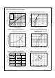
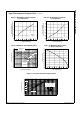
•
0.2 A, 600 V, R
DS(on)
=9.3
Ω(7\S.)@V
GS
=10 V, I
D
=0.1 A
• Low Gate Charge (Typ. nC)
•
Low C
rss
(Typ. pF)
•
100% Avalanche Tested
N-Channel QFET
®
MOSFET
600V, 0.2 A, 11.5 Ω
Description
•
RoHS Compliant