
Datasheet


©2007 Fairchild Semiconductor Corporation www.fairchildsemi.com
H11G1M, H11G2M, H11G3M Rev. 1.0.4 2
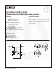
H11G1M, H11G2M, H11G3M — High Voltage Photodarlington Optocouplers
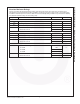
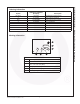
Absolute Maximum Ratings
Stresses exceeding the absolute maximum ratings may damage the device. The device may not function or be
operable above the recommended operating conditions and stressing the parts to these levels is not recommended.
In addition, extended exposure to stresses above the recommended operating conditions may affect device reliability.
The absolute maximum ratings are stress ratings only.
Symbol Parameter Value Units
TOTAL DEVICE
T
STG
Storage Temperature -40 to +150 °C
T
OPR
Operating Temperature -40 to +100 °C
T
SOL
Lead Solder Temperature (Wave Solder) 260 for 10 sec °C
P
D
Total Device Power Dissipation @ T
A
= 25°C 260 mW
Derate Above 25°C 3.5 mW/°C
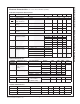
EMITTER
I
F
Forward Input Current 60 mA
V
R
Reverse Input Voltage 6.0 V
I
F
(pk) Forward Current – Peak (1µs pulse, 300pps) 3.0 A
P
D
LED Power Dissipation @ T
A
= 25°C 100 mW
Derate Above 25°C 1.8 mW/°C
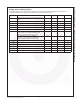
DETECTOR
V
CEO
Collector-Emitter Voltage
V
H11G1M 100
H11G2M 80
H11G3M 55
P
D
Photodetector Power Dissipation @ T
A
= 25°C 200 mW
Derate Above 25°C 2.67 mW/°C