
Datasheet

©2005 Fairchild Semiconductor Corporation www.fairchildsemi.com
H11L1M, H11L2M, H11L3M Rev. 1.0.6 2
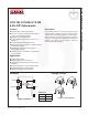
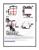
H11L1M, H11L2M, H11L3M — 6-Pin DIP Optocoupler
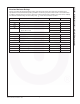
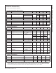
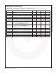
Absolute Maximum Ratings
Stresses exceeding the absolute maximum ratings may damage the device. The device may not function or be
operable above the recommended operating conditions and stressing the parts to these levels is not recommended.
In addition, extended exposure to stresses above the recommended operating conditions may affect device reliability.
The absolute maximum ratings are stress ratings only.
T
A
= 25°C unless otherwise specified.
Symbol Parameters Value Units
Total Device
T
STG
Storage Temperature -40 to +150 °C
T
OPR
Operating Temperature -40 to +85 °C
T
SOL
Lead Solder Temperature 260 for 10 seconds °C
P
D
Total Device Power Dissipation at 25°C 250 mW
Derate Above 25°C 2.94 mW/°C
Emitter
I
F
Continuous Forward Current 30 mA
V
R
Reverse Voltage 6 V
I
F
(pk) Forward Current – Peak (1 µs pulse, 300 pps) 100 mA
P
D
LED Power Dissipation 60 mW
Detector
P
D
Detector Power Dissipation 150 mW
V
O
V
45
Allowed Range 0 to 16 V
V
CC
V
65
Allowed Range 3 to 16 V
I
O
I
4
Output Current 50 mA