
Datasheet

©2008 Fairchild Semiconductor Corporation www.fairchildsemi.com
6N13XM, HCPLXXXM Rev. 1.0.12 3
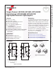
Single-Channel: 6N135M, 6N136M, HCPL4503M
Dual-Channel: HCPL2530M, HCPL2531M — High Speed Transistor Optocouplers
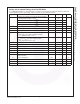
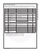
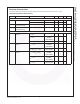
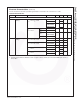
Absolute Maximum Ratings
Stresses exceeding the absolute maximum ratings may damage the device. The device may not function or be
operable above the recommended operating conditions and stressing the parts to these levels is not recommended.
In addition, extended exposure to stresses above the recommended operating conditions may affect device reliability.
The absolute maximum ratings are stress ratings only.
T
A
= 25°C unless otherwise specified.
Notes:
1. Derate linearly above 70°C free-air temperature at a rate of 0.8 mA/°C.
2. Derate linearly above 70°C free-air temperature at a rate of 1.6 mA/°C.
3. Derate linearly above 70°C free-air temperature at a rate of 0.9 mW/°C.
4. Derate linearly above 70°C free-air temperature at a rate of 2.0 mW/°C.
Symbol Parameter Condition Value Units
T
STG
Storage Temperature -40 to +125 °C
T
OPR
Operating Temperature -40 to +100 °C
T
SOL
Lead Solder Temperature 260 for 10 s °C
EMITTER
I
F
(avg) DC/Average Forward Input
Current Each Channel
(1)
25 mA
I
F
(pk) Peak Forward Input Current
Each Channel
(2)
50% Duty Cycle, 1 ms P.W. 50 mA
I
F
(trans) Peak Transient Input Current
Each Channel
≤
1 µs P.W., 300 pps 1.0 A
V
R
Reverse Input Voltage Each
Channel
5V
P
D
Input Power Dissipation Each
Channel
(3)
6N135M, 6N136M, and HCPL4503M 45 mW
HCPL2530M and HCPL2531M
DETECTOR
I
O
(avg) Average Output Current Each
Channel
8 mA
I
O
(pk) Peak Output Current Each
Channel
16 mA
V
EBR
Emitter-Base Reverse Voltage 6N135M and 6N136M 5 V
V
CC
Supply Voltage -0.5 to 30 V
V
O
Output Voltage -0.5 to 20 V
I
B
Base Current 6N135M and 6N136M 5 mA
PD Output Power Dissipation
Each Channel
(4)
6N135M, 6N136M, and HCPL4503M 100 mW
HCPL2530M and HCPL2531M 35 mW