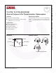
TIL111M, TIL117M, MOC8100M General Purpose 6-Pin Phototransistor Optocouplers Features General Description ■ UL Recognized (File # E90700) The MOC8100M, TIL111M, and TIL117M optocouplers consist of a gallium arsenide infrared emitting diode driving a silicon phototransistor in a 6-pin dual in-line package. ■ VDE Recognized (File #102497 for white package) – Add Option V (e.g.
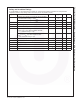
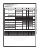
Symbol Parameter Min. Typ. Max. Unit Installation Classifications per DIN VDE 0110/1.89 Table 1 For Rated Mains Voltage < 150 VRMS I–IV For Rated Mains Voltage < 300 VRMS I–IV Climatic Classification 55/100/21 Pollution Degree (DIN VDE 0110/1.89) 2 CTI Comparative Tracking Index 175 VPR Input to Output Test Voltage, Method b, VIORM x 1.875 = VPR, 100% Production Test with tm = 1 s, Partial Discharge < 5 pC 1594 Input to Output Test Voltage, Method a, VIORM x 1.
Symbol Parameter Device Value Units -40 to +150 °C Total Device TSTG Storage Temperature All TOPR Operating Temperature All -40 to +100 °C TSOL Lead Solder Temperature All 260 for 10 sec °C Total Device Power Dissipation @ TA = 25°C All 250 mW 2.
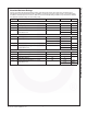
Individual Component Characteristics Symbol Parameter Test Conditions Device Min. Typ.* Max. Unit Emitter VF IR Input Forward Voltage Reverse Leakage Current IF = 16 mA TA = 25°C IF = 10 mA for MOC8100M, IF = 16 mA for TIL117M TA = 0°C to 70°C TA = -55°C TIL111M 1.2 1.4 MOC8100M, TIL117M 1.2 1.4 V 1.32 TA = +100°C 1.10 VR = 3.0 V TIL111M, TIL117M 0.001 10 µA VR = 6.0 V MOC8100M 0.001 10 µA Detector BVCEO Collector-Emitter Breakdown Voltage IC = 1.
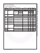
TA = 25°C unless otherwise specified. Transfer Characteristics Symbol Parameter Test Conditions Device Min Typ* Max Unit IF = 10 mA, VCE = 10 V TIL117M 50 % MOC8100M 50 % DC Characteristics CTRCE Current Transfer Ratio, Collector to Emitter IF = 1 mA, VCE = 5 V 30 IF = 1 mA, VCE = 5 V, TA = 0°C to +70°C IC(ON) On-State Collector Current (Phototransistor Operation) IF = 16 mA, VCE = 0.4 V On-State Collector Current (Photodiode Operation) IF = 16 mA, VCB = 0.
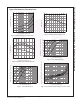
1.8 1.6 VCE = 5.0 V TA = 25˚C 1.7 1.6 Normalized to IF = 10 mA 1.2 1.5 1.0 NORMALIZED CTR VF – FORWARD VOLTAGE (V) 1.4 1.4 TA = -55°C 1.3 TA = 25°C 1.2 0.8 0.6 0.4 TA = 100°C 0.2 1.1 0.0 1.0 1 10 0 100 2 4 6 8 10 12 14 16 18 20 IF – FORWARD CURRENT (mA) IF – LED FORWARD CURRENT (mA) Figure 4. Normalized CTR vs. Forward Current Figure 3. LED Forward Voltage vs. Forward Current NORMALIZED CTR ( CTRRBE / CTRRBE(OPEN)) 1.4 1.2 IF = 5 mA NORMALIZED CTR 1.0 IF = 10 mA 0.
1000 IF = 10 mA VCC = 10 V TA = 25˚C NORMALIZED ton – (ton(RBE) / ton(open)) 5.0 SWITCHING SPEED (μs) 100 Tf Toff 10 Ton Tr 1 VCC = 10 V IC = 2 mA RL = 100 Ω 4.5 4.0 3.5 3.0 2.5 2.0 1.5 1.0 0.5 10 100 0.1 0.1 1 10 1000 10000 100000 RBE – BASE RESISTANCE (kΩ) 100 R – LOAD RESISTOR (kΩ) Figure 10. Normalized ton vs. RBE Figure 9. Switching Speed vs. Load Resistor ICEO – COLLECTOR -EMITTER DARK CURRENT (nA) NORMALIZED toff – (toff(RBE) / toff(open)) 1.4 1.3 1.2 1.1 1.0 0.9 0.8 0.7 0.
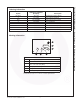
TIL111M, TIL117M, MOC8100M — General Purpose 6-Pin Phototransistor Optocouplers Reflow Profile 300 260°C 280 260 >245°C = 42 s 240 220 200 180 °C Time above 183°C = 90 s 160 140 120 1.822°C/s Ramp up rate 100 80 60 40 33 s 20 0 0 60 120 180 270 360 Time (s) Figure 14. Reflow Profile ©2005 Fairchild Semiconductor Corporation TIL111M, TIL117M, MOC8100M Rev. 1.0.3 www.fairchildsemi.
Option Order Entry Identifier (Example) No option TIL111M S TIL111SM SR2 TIL111SR2M T TIL111TM 0.4" Lead Spacing V TIL111VM VDE 0884 TV TIL111TVM VDE 0884, 0.
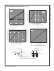
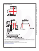
TIL111M, TIL117M, MOC8100M — General Purpose 6-Pin Phototransistor Optocouplers Package Dimensions Figure 15. 6-Pin DIP Through Hole Package drawings are provided as a service to customers considering Fairchild components. Drawings may change in any manner without notice. Please note the revision and/or date on the drawing and contact a Fairchild Semiconductor representative to verify or obtain the most recent revision.
TIL111M, TIL117M, MOC8100M — General Purpose 6-Pin Phototransistor Optocouplers Package Dimensions (Continued) Figure 16. 6-Pin DIP Surface Mount Package drawings are provided as a service to customers considering Fairchild components. Drawings may change in any manner without notice. Please note the revision and/or date on the drawing and contact a Fairchild Semiconductor representative to verify or obtain the most recent revision.
TIL111M, TIL117M, MOC8100M — General Purpose 6-Pin Phototransistor Optocouplers Package Dimensions (Continued) Figure 17. 6-Pin DIP 0.4” Lead Spacing Package drawings are provided as a service to customers considering Fairchild components. Drawings may change in any manner without notice. Please note the revision and/or date on the drawing and contact a Fairchild Semiconductor representative to verify or obtain the most recent revision.
12.0 ± 0.1 4.5 ± 0.20 2.0 ± 0.05 0.30 ± 0.05 4.0 ± 0.1 Ø1.5 MIN 1.75 ± 0.10 11.5 ± 1.0 21.0 ± 0.1 9.1 ± 0.20 0.1 MAX 10.1 ± 0.20 24.0 ± 0.3 Ø1.5 ± 0.1/-0 User Direction of Feed Figure 18. Carrier Tape Specification ©2005 Fairchild Semiconductor Corporation TIL111M, TIL117M, MOC8100M Rev. 1.0.3 www.fairchildsemi.
TIL111M, TIL117M, MOC8100M — General Purpose 6-Pin Phototransistor Optocouplers ©2005 Fairchild Semiconductor Corporation TIL111M, TIL117M, MOC8100M Rev. 1.0.3 www.fairchildsemi.