PRELIMINARY OSPREY CAMERA SERIES CAM/CCD-2KLV.TDI CAM/CCD-4KLV.
PRELIMINARY FAIRCHILD IMAGING OSPREY CAMERA SERIES USER’S MANUAL CAM/CCD-2KLV.TDI and CAM/CCD-4KLV.TDI Rev 073004 © 2004 Fairchild Imaging, Inc. Fairchild Imaging, Inc. 1801 McCarthy Blvd. Milpitas CA 95035 1-800-325-6975 www.fairchildimaging.com PRELIMINARY DOCUMENT The information in this manual is preliminary. All information provided in this manual is believed to be correct at the time of writing. No responsibility is assumed by Fairchild Imaging for its use.
PRELIMINARY Table of Contents SECTION 1 Introduction to the CAM/CCD-2KLV.TDI and CAM/CCD-4KLV.TDI High Performance TDI Line Scan Camera ...................................................................... 5 1.1 1.2 1.3 1.4 1.5 1.6 1.7 1.8 Camera Highlights ....................................................................................................... 5 Camera Specification................................................................................................... 6 Image Sensor...........
PRELIMINARY SECTION 5 Handling Instructions ....................................................................................................... 31 5.1 5.2 5.3 5.4 Electrostatic Discharge ................................................................................................ 31 Preventing ESD Damage............................................................................................. 31 Protecting Against Dust, Oil and Scratches ...........................................................
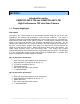
PRELIMINARY SECTION 1 Introduction to the CAM/CCD-2KLV.TDI and CAM/CCD-4KLV.TDI High Performance TDI Line Scan Camera 1.1 Camera Highlights Description The Osprey TDI camera series is an ultra-sensitive camera design for use in line scan applications that demand high performance under low light conditions. This series of cameras is based upon Fairchild’s CCD525 array, which is used in the very successful U.S. Postal Service Wide Field of View (WFOV) Camera.
PRELIMINARY Programmability Simple menu-based configuration for selection of gain, offset operational control, and diagnostics. • LVDS camera-PC communications with Fairchild-supplied user GUI. Usability Programmable gain, offsets, and controls. • Easy integration “plug compatabile” LVDS hookup Full Spectrum of Applications • • • • • Precision manufacturing inspection Web inspection Sorting and routing Biomedical readout systems Diagnostic systems 1.2 Camera Specification – CAM/CCD-2KLV.
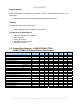
PRELIMINARY Notes: DN = Digital Numbers, also known as “levels” (0 – 255 for 8-bit systems, 0 – 4095 for 12-bit systems). All measurements taken with camera operating in 96 stage mode. All measurements exclude the last pixel of OS 1 and the first pixel of OS4. Tested using volpi (18111.001) linght line source, default camera gain. 1. Measured across 1 tap (512 pixels – 2K) (1024 pixels – 4K). 2. Typical offset @ 20°C ambient. 3. Excludes last pixel of OS1 and first pixel. 4. Measured across all taps. 5.
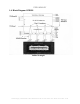
PRELIMINARY 1.4 Block Diagram CCD525 2048 x 96 stages Fairchild Imaging • CAM/CCD-2KLV.TDI & CAM/CCD-4KLV.
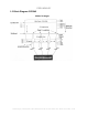
PRELIMINARY 1.5 Block Diagram CCD545 4096 x 96 stages Fairchild Imaging • CAM/CCD-2KLV.TDI & CAM/CCD-4KLV.
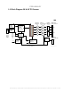
PRELIMINARY 1.6 Block Diagram 2K & 4K TDI Camera DC B IA S SUPP. . . . . . . . . J4 In p u t Power + 1 2 .0 V GND + 5 .2 G E N ’L PW R SUPP. +14V 2 5 .0 M H z H i Speed C lo c k D r iv e r s O u tp u ts + 3 .3 + 3 .3 CCD Sensor 5 T im in g & I / O C o n t ro l 50M H z M a s te r C lo c k + 3 .0 A + 3 .3 D + 3 .3 D 4 4 / 8 / 8 3 3 / 8 / 8 2 2 / 8 / 8 1 1 / 8 / 8 SHP SHD / +14V +10V + 5 .2 A + 5 .0 D + 3 .3 D + 3 .
PRELIMINARY 1.7 2K/4K TDI Camera Timing Diagram Note: Timing diagram not to scale 2K TDI LVDS Strobe period LVAL set-up time Line period (min.) Blanking ExSync min pulse width :40 nS :20 nS :21.8 uS :0.8 uS :120 ns 4K TDI LVDS Strobe period LVAL set-up time Line period (min.) Blanking ExSync min pulse width :40 nS :20 nS :43.1 uS :2.15 uS :120 ns Fairchild Imaging • CAM/CCD-2KLV.TDI & CAM/CCD-4KLV.
PRELIMINARY 1.8 Thermal Considerations The Osprey camera series has been thermally designed to separate the camera electronics from the image sensor. The sensor temperature is thermally linked near the four M4 mounting holes on the face of the camera. Fairchild Imaging recommends mounting the camera using these holes to minimize sensor dark current artifacts. Fairchild Imaging recommends that gain or offset corrections are completed after the camera has been turned on for at least 15 minutes.
PRELIMINARY SECTION 2 Camera Hardware Interface 2.1 Installation Overview Before you integrate your camera into your system you should first determine some basic operating parameters such as what resolution you need. Do you know the speed of the object that your camera will be inspecting? One additional point you want to keep in mind is your lighting requirement.
PRELIMINARY 2.2 Connectors, Pinouts, and Cables 2.2.1 CONTROL-DB15 Connector, Amphenol Hood 17-1657-15 AMP Receptable 205205-2 Camera Pin # 12 4 5 13 14 6 8 7 10 2 9 11 1 15 Signal Name +ExSync -ExSync +FrameSel -FrameSel +TDISEL0 -TDISEL0 +TDISEL1 -TDISEL1 SCLK S Data In SLOAD RESETIN S Data Out GND Fairchild Imaging • CAM/CCD-2KLV.TDI & CAM/CCD-4KLV.
PRELIMINARY 2.2.2 LVDS Data, J7 & J8 connector, 3M 10140-6000EC connector, 3M 103403210-000 hood or equivilent.
PRELIMINARY 2.3 Power Supply The camera uses a single voltage input, normally set to 12 volts @ 0.7 Amps typ., supplied through a Hirose connector. The supply must support a 850mA current surge for 100ms for proper camera operation. Ripple and noise is required to be < 50 mV RMS for best camera noise performance. Cable construction with shielded and grounded shields is required. Hirose HR25-7TR-6P Receptacle Pin # Description 1 +12V 2 +12V 3 NC 4 GND 5 GND 6 NC 2.
PRELIMINARY SECTION 3 Camera Control 3.1 Quick Start with LVDS Interface Follow your frame grabber manufacturer’s instructions when inserting the frame grabber card into your PC. Be sure that you install the correct configuration software that matches the camera that you are using. Fairchild Imaging supplies configuration files for each camera type. To enter into the realtime display, place your cursor in the window and hit return.
PRELIMINARY 3.3 Providing External Triggering There are two ways to provide external triggering to the 2K & 4K TDI LVDS cameras: • • 3.3.1 Directly send the external trigger to the camera’s DB15 connector as mentioned earlier. Provide an external trigger to the frame grabber and it will send the EXSYNC signal to the camera. Direct Trigger In this configuration, the EXSYNC is sent directly to the camera from the external LVDS trigger source (frame grabber, shaft encoder, etc.). 3.3.
PRELIMINARY 3.2.3 TTL Trigger Source If the external trigger source is a TTL level, the signal needs to be converted to a LVDS signal before sending it to the camera. An example of this circuit is illustrated below: J5 U1 1 7 9 15 EXT. TRIGGER 4 12 +3.3 16 C1 .1uF 8 DI1 DI2 DI3 DI4 EN1/2 EN3/4 VCC GND DO1+ DO1DO2+ DO2DO3+ DO3DO4+ DO4- 2 3 EXSY NC + EXSY NC - 6 5 10 11 14 13 12 4 SN65LVDS3487/SO DSUB 15-P TTL TRIGGER SOURCE 3.
PRELIMINARY GROUND EXTERNAL TRIGGER (TTL) J3 CAMERA CONNECTOR 95 J5 100 33 AMP 100 24 FRAME GRABBER CONNECTOR EXSYNC + EXSYNC - 12 4 DSUB 15-P AMP 100 3.5 Frame Mode Framing mode is an excellent tool for mechanical and optical aligning of the camera to the target. Frame mode is available in master mode only and the line rate is fixed at 23.19 KHz. The circuit is shown on the following page. Fairchild Imaging • CAM/CCD-2KLV.TDI & CAM/CCD-4KLV.
PRELIMINARY WIRING CONNECTION +USER I/O +FRAME SEL (pin 5) CAM DB15 -FRAME SEL (pin 13) -USER I/O F R A M E G R A B B E R CAM +VSYNC + FVAL (pin 20) -VSYNC - FVAL (pin 45) +HSYNC -LVALB (pin 20) J7 CAM J8 -HSYNC -LVALB (pin 45) Fairchild Imaging • CAM/CCD-2KLV.TDI & CAM/CCD-4KLV.
PRELIMINARY 3.6 System Connection F R A M E LED TRIGGER (Inverted FRAME SEL) VOLPI 18111.001 LED Driver FRAME SEL SIGNAL CAM HSYNC G R A B B E R VSYNC LED Array T A R G E T How to operate in framing mode 1. The camera must be running in master mode. • External sync signal cannot be present at power up. 2. Provide a LVDS active low “FRAME SEL” LVDS signal to pin 5 and pin 13 of the camera’s control connector (DB15). READOUT TIME EXPOSURE TIME FRAME PULSE 1.
PRELIMINARY 3.7 TDI Length Selection TDI length selection for the 2K/4KTDI LVDS camera can be selected using the combination of TDISEL0 and TDISEL1 input signal into the DB15 control connector. The TDISEL0 and TDISEL1 are LVDS level signals. They are typically wired to the user control I/O of the frame grabber. For 2K / 4KTDI LVDS cameras, the TDI lengths are available for 96, 64, 32 and 16.
PRELIMINARY 3.8 Gain and Offset Calibration Gain and offset calibration are supported with use of the "FI LVDS Camera Control" graphic user interface (GUI). Note: When saving directly into ROM, stored values are not applied until after power cycle. Values written to RAM are implemented immediately. 3.9 How to Modify Gain & Offset Values 1. Read the data stored in the ROM and record the factory adjusted values. 2. Enter the gain changes for CH1 through CH4. 3. Write the changes to the RAM.
PRELIMINARY 3.10 Data Bus The 2K and 4K TDI cameras have 4 channels of 8-bit digital data in RS-644 (LVDS) format. See Reference B of this manual for detailed information on RS644. Both 2K and 4K TDI cameras output the clocking signals STROBE and LVAL. 3.10.1 STROBE STROBE is an internal pixel clock inside the camera (fixed at 25 MHz) data rate. To acquire valid data, frame grabbers usually latch to the rising edge of STROBE with LVAL high. 3.10.
PRELIMINARY SECTION 4 Mechanical and Optical Considerations 4.1 Camera Dimensions and Mounting The 2K and 4K TDI camera housings are manufactured with high precision. alignment is to the four M4 face mounting holes. Sensor The 2K and 4K TDI camera housings are equipped with four M4 mounting holes on the front and two M4 mounting holes on one side and on the bottom of the camera. Use caution in the following ways to avoid stripping threads or stressing the case: • Use only M4 screws.
PRELIMINARY 4.2 Lenses The 2K and 4K TDI cameras as shipped from the factory accept M58 optical components with M58 threads. The 4K TDI camera only accepts M58 lens types. A sample lens system for 256 DPI would include the following: 40mm lens, Schneider P/N 25-014798 Folus Mount, Schneider P/N 21-013048 Adapter, Schneider P/N 25-020054 When the lens mount (lens extender tube and its lock ring) is removed, the front surface of the camera is seen as a square with a large threaded hole in the center.
PRELIMINARY 4.3 Mechanical Drawing of Optional Camera Face Mounting “L” Bracket Contact your Fairchild Imaging representative for more details. 4.4 Lenses Fairchild Imaging does not supply lenses. An example lens setup is detailed in Section 4.2 above. Fairchild Imaging • CAM/CCD-2KLV.TDI & CAM/CCD-4KLV.
PRELIMINARY 4.5 Positioning Accuracy of the Sensor Chip in the Camera Position accuracy of the sensor chip in the horizontal and vertical direction is + 2 mils. Rotational positioning accuracy is as shown. Reference position is the center-line of the four M4 mounting holes of the camera housing. Since the translatory and rotational positioning tolerance depend on each other, the worse case of maximum rotational and horizontal/vertical mis-positioning can not occur at the same time. 4.
PRELIMINARY 4.8 Lens Modeling Several camera companies have included this and like information in their manuals. For reference material it is very useful. The focal point is the point at which the image of an infinitely distant object is brought to focus. The effective focal length (f’) is the distance from the second principal point to the second focal point. The back focal length (BFL) is the distance from the image side of the lens surface to the second focal point.
PRELIMINARY SECTION 5 Handling Instructions 5.1 Electrostatic Discharge The Fairchild Imaging Osprey camera uses TDI technology in a CCD base, and as all such devices, has some limited inherent susceptibility to electrostatic discharge (ESD). All reasonable and customary design steps have been taken to provide ESD protection circuitry.
PRELIMINARY SECTION 6 Troubleshooting 6.
PRELIMINARY Everything Seems to be Working, But No Image Remove the cover from your PC and reset all the cards into the mother board. Sometimes when you move your PC, cards inside the PC work themselves loose. Don’t forget to check for optical path obscuration also. Data Clocking/Output Signals Verify the presence of all data clocking and output signals at the connector pins on the camera housing.
PRELIMINARY Look at your light source. Keep in mind that it is better on the side of too much light rather than too little. Excess light allows internal gain reduction in the camera which, in turn, improves camera dynamic range. Also, if your light source is AC instead of DC this will make the image look noisy. If the object you are inspecting has different surface textures it can produce an image that may look noisy.
PRELIMINARY SECTION 7 Product Support If, after troubleshooting your camera, you are still having problems, collect the following data about your application and call Fairchild Imaging Customer Support. Note: You may also want to photocopy this fax page for sending information to Fairchild Imaging @ 408-735-7352 Your Name Company name Your phone number Your Fax number Product Model Number (e.g.
PRELIMINARY REFERENCE A Providing External Trigger Using PCI-1424 Frame Grabber 1.
PRELIMINARY REFERENCE B Introduction to LVDS National Semiconductor first introduced LVDS as a standard in 1994. National recognized that the demand for bandwidth was increasing at an exponential rate while users also desired low power dissipation. This exceeded the speed capabilities of RS-422 and RS485 differential transmission standards.
PRELIMINARY The LVDS Standard LVDS is currently standardized by the TIA/EIA (Telecommunications Industry Association/Electronic Industries Association) ANSI/TIA/EIA-644-A (LVDS) Standard. The generic (multi-application) LVDS standard, ANSI/TIA/EIA-644-A, began in the TIA Data Transmission Interface committee TR30.2 in 1995. It was revised and published as ANSI/TIA/EIA-644-A in 2001. The ANSI/TIA/EIA standard defines driver output and receiver input characteristics, thus it is an electrical-only standard.