
Data Sheet
FSC-BT1006A Datasheet
Shenzhen Feasycom Technology Co.,Ltdwww.feasycom.com
-31-
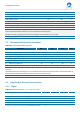
5V(VCC_CHG)
-0.4
+5.75 / 6.50
(a)
V
BATTERY(LED 0,1,2)
-0.4
+4.4
V
BATTERY(VBAT_IN)
-0.4
+4.4
V
BATTERY(VREGENABLE)
-0.4
+4.4
V
VDD_USB/3.3V_OUT
-0.4
+3.6
V
VDD_IO
-0.4
+3.6
V
Other terminal voltages
VSS-0.4
VDD+0.4≤3.60
(b)
V
T
ST
- Storage Temperature
-40
+105
°C
(a) Standard maximum input voltage is 5.75V, a 6.50V maximum depends on firmware version and implementation of
over-temperatureprotection software, for more information contact Feasycom.
(b) VDD is the VDD_IO supply domain for this I/O. Voltage must not exceed 3.6 V on any I/O.
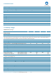
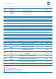
5.2 Recommended Operating Conditions
Table 15:Recommended Operating Conditions
Parameter
Min
Type
Max
Unit
5V(VCC_CHG)
4.75 / 3.10 (a)
5
5.75 / 6.50 (b)
V
BATTERY(LED 0,1,2)
1.10
3.70
4.30
V
BATTERY(VBAT_IN)
2.8
3.3
4.30
V
BATTERY(VREGENABLE)
0
3.3
4.25
V
VDD_USB/3.3V_OUT
3.1
3.3
3.6
V
VDD_IO
1.7
1.8
3.6
V
T
A
- Operating Temperature
-40
20
+85
°C
(a) Minimum input voltage of 4.75V is required for full specification, regulator operates at reduced load current
from3.1V
(b) Standard maximum input voltage is 5.75V, a 6.50V maximum depends on firmware version and implementation of
over-temperatureprotection software, for more information contact Feasycom.
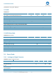
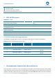
5.3 Input/output Terminal Characteristics
5.3.1 Digital
Table 16: DC Characteristics (V
DD
- V
SS
= 3 ~ 3.6 V, T
A
= 25C)
Parameter
Min
Type
Max
Unit
Input Voltage
V
IL
- Standard IO Low levelinput voltage
-0.4
-
0.4
V
V
IH
- Standard IO Low levelinput voltage
0.7XVDD_IO
-
VDD_IO+0.4
V
Tr/Tf
-
-
25
nS