
Data Sheet

FSC-BT1006A Datasheet
Shenzhen Feasycom Technology Co.,Ltdwww.feasycom.com
-40-
9. HARDWARE INTEGRATION SUGGESTIONS
9.1 Soldering Recommendations
FSC-BT1006A is compatible with industrial standard reflow profile for Pb-free solders. The reflow profile used is
dependent on the thermal mass of the entire populated PCB, heat transfer efficiency of the oven and particular type of
solder paste used. Consult the datasheet of particular solder paste for profile configurations.
Feasycom will give following recommendations for soldering the module to ensure reliable solder joint and operation of
the module after soldering. Since the profile used is process and layout dependent, the optimum profile should be
studied case by case. Thus following recommendation should be taken as a starting point guide.
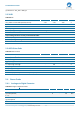
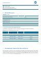
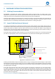
9.2 Layout Guidelines(Internal Antenna)
It is strongly recommended to use good layout practices to ensure proper operation of the module. Placing copper or
any metal near antenna deteriorates its operation by having effect on the matching properties. Metal shield around the
antenna will prevent the radiation and thus metal case should not be used with the module. Use grounding vias
separated max 3 mm apart at the edge of grounding areas to prevent RF penetrating inside the PCB and causing an
unintentional resonator. Use GND vias all around the PCB edges.
The mother board should have no bare conductors or vias in this restricted area, because it is not covered by stop mask
print. Also no copper (planes, traces or vias) are allowed in this area, because of mismatching the on-board antenna.
5
26.9
Max.0.5
20
10
43.5
13
18
Max.0.5
10
20
Applic. PCB
no bare copper(exept solder pads for module)
no copper and components on any layer
no components on any layer
do not place any conductive parts in this area
Provide solid ground plane(s) as large as possible around area
Figure 21:FSC-BT1006A Restricted Area
Following recommendations helps to avoid EMC problems arising in the design. Note that each design is unique and the
following list do not consider all basic design rules such as avoiding capacitive coupling between signal lines. Following
list is aimed to avoid EMC problems caused by RF part of the module. Use good consideration to avoid problems arising
from digital signals in the design.
Ensure that signal lines have return paths as short as possible. For example if a signal goes to an inner layer through a
via, always use ground vias around it. Locate them tightly and symmetrically around the signal vias. Routing of any
sensitive signals should be done in the inner layers of the PCB. Sensitive traces should have a ground area above and
under the line. If this is not possible, make sure that the return path is short by other means (for example using a
ground line next to the signal line).