
Data Sheet


FSC-BT1006A Datasheet
Shenzhen Feasycom Technology Co.,Ltdwww.feasycom.com
-41-
9.3 Layout Guidelines(External Antenna)
Placement and PCB layout are critical to optimize the performances of a module without on-board antenna designs.
The trace from the antenna port of the module to an external antenna should be 50 and must be as short as possible
to avoid any interference into the transceiver of the module. The location of the external antenna and RF-IN port of
the module should be kept away from any noise sources and digital traces. A matching network might be needed in
between the external antenna and RF-IN port to better match the impedance to minimize the return loss.
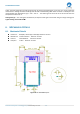
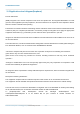
As indicated in Figure below, RF critical circuits of the module should be clearly separated from any digital circuits on
the system board. All RF circuits in the module are close to the antenna port. The module, then, should be placed in
this way that module digital part towards your digital section of the system PCB.
Antenna
RF_IN
Digital Part
Non enmitting
circuits
Non enmitting
circuits
Digital & Analog Circuits
PCB
Antenna
RF & heat
enmitting
circuits
Digital Part
RF_IN
Digital & Analog Circuits
RF & heat
enmitting
circuits
PCB
Figure 22: Placement the Module on a System Board
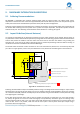
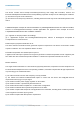
9.3.1 Antenna Connection and Grounding Plane Design
Antenna
Matching
Network
5mm
RF_IN
Figure 23: Leave 5mm Clearance Space from the Antenna
General design recommendations are:
The length of the trace or connection line should be kept as short as possible.
Distance between connection and ground area on the top layer should at least be as large as the dielectric
thickness.
Routing the RF close to digital sections of the system board should be avoided.