
Data Sheet


FSC-BT958 Datasheet
Shenzhen Feasycom Technology Co., Ltd www.feasycom.com
-6-
27 28 29 30
31
21
20
19
18
17
16
35
36
37
38
39
NC
GPIO_03/I2S_CLK
NC
VCC_CHG
NC
NC
NC
33
34
15
14
NC
VREGENABLE
DEBUG_TX/I2C_DAT
NC
NC
NC
LED0
LED1
LED2
GND
GPIO_02/I2S_DO
GPIO_00/I2S_DI
GPIO_01/I2S_WS
NC
EXT_ANT
32
2523 2422
VBAT_IN
BT_TX
BT_RX
MIC_N
MIC_P
NC
SPK_LP
SPK_LN
NC
NC
SPK_RN
SPK_RP
13
12
11
10
9
8
7
6
5
4
3
2
1
43
44
45
46
47
41
42
40
51
52
49
50
48
NC
GND GND
GND
GPIO_03/I2S_CLK
GPIO_10/BT_CTS
GPIO_11/BT_RTS
27
26
GPADC1
GND
NC
DEBUG_RX/I2C_CLK
NC
NC
MIC_BIAS
GPIO_00/I2S_DI
GPIO_02/I2S_DO
GPIO_01/I2S_WS
RESET
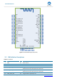
Figure 3: FSC-BT958 PIN Diagram(Top View)
3.2 PIN Definition Descriptions
Table 2: Pin definition
Pin
Pin Name
Type
Pin Descriptions
1
GND
Vss
Power Ground
2
NC
3
NC
4,12
GPIO_03/I2S_CLK
I/O
Programmable input/output line
Alternative Function: I2S2 synchronous data clock
5,10
GPIO_00/I2S_DI
I/O
Programmable input/output line
Alternative Function: I2S2 synchronous data input
6,11
GPIO_02/I2S_DO
I/O
Programmable input/output line