LC116-LA Hardware Guide V1.
Copyright Statement Copyright © 2022 Fibocom Wireless Inc. All rights reserved. Without the prior written permission of the copyright holder, any company or individual is prohibited to excerpt, copy any part of or the entire document, or distribute the document in any form. Note The document is subject to update from time to time owing to the product version upgrade or other reasons. Unless otherwise specified, the document only serves as the user guide.
Contents Contents Applicability Type............................................................................................... 4 Change History .................................................................................................. 5 1 Overview .......................................................................................................... 6 1.1 Product Introduction ................................................................................................... 6 1.
Contents 4.2.2 Auto power-on ...................................................................................................... 37 4.2.3 Power-off ................................................................................................................ 38 4.2.4 Reset ........................................................................................................................ 39 4.3 Operating Mode .........................................................................................
Contents 4.4.11 SGMII .................................................................................................................... 57 4.5 RF Part ........................................................................................................................... 58 4.5.1 Antenna Design .................................................................................................... 58 4.5.2 Impedance Design ..................................................................................
Applicability Type Applicability Type No. Applicability Type 1 LC116-LA Description MCP is 2Gbit Flash+2Gbit RAM, and supports MAIN_ANT and DIV_ANT. Copyright © Fibocom Wireless Inc.
Change History Change History V1.0 (2021-11-10) Initial version V1.1 (2021-12-16) Updated the known issues. Copyright © Fibocom Wireless Inc.
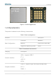
1 Overview 1 Overview 1.1 Product Introduction The LC116-LA module is a broadband wireless terminal product based on Qualcomm 9X07 platform, applicable to multiple network systems and bands such as TDD-LTE, FDD-LTE, WCDMA and GSM. The following table lists the sub-models of the LC116-LA product. Table 1. Sub-models of the LC116-LA product No.
1 Overview Figure 1. Product appearance 1.2 Characteristics The product hardware has the following characteristics. Table 2. Basic configuration Indicator Basic Configuration Description Processor MDM9X07 Memory 2Gbit Flash+2Gbit RAM Supported Operating System LINUX Table 3. Baseband characteristics Category Description USB × 1, support USB2.
1 Overview PCM × 1 SD × 1 ADC × 3 Table 4. RF characteristics Category Antenna interface Description Main antenna × 1 Diversity antenna × 1 1.3 System architecture The LC116-LA product hardware consists of the following parts: Baseband part: PMIC, MCP, USB, (U)SIM, PCM, I2C, UART, SGMII, SDIO, GPIOs, GSM/CDMA/EVDO/WCDMA/TD-SCDMA/LTE TDD/LTE FDD controller RF part: RF Transceiver, RF PA, RF filter Antenna The following figure shows the internal structural block diagram. 1.
1 Overview Operating Mode Description module is powered on. The module is powered on and successfully registered with the network for service transmission. The module can be operated using Transmission the AT commands through the serial port. The module transmits data. When data transmission is completed, the module returns to the standby or low-power mode. The module is in light sleep state. It is connected to a network and Sleep can receive paging messages.
2 Technical Indicators 2 Technical Indicators 2.1 Physical Indicators Table 6. LC116-LA package mode Indicator Description Weight 5.2 g Package LCC+LGA 143 Pin Appearance dimensions (30.0±0.15) mm × (30.0±0.15) mm × (2.4±0.2) mm Structural dimensions See the figure below. The following figure shows the structural dimensions. Copyright © Fibocom Wireless Inc.
2 Technical Indicators Figure 2. Structural dimensions 2.2 RF Table 7.
2 Technical Indicators System Band Description Tx (MHz) Rx (MHz) LTE FDD Band 28 IMT 700 703–748 758-803 LTE TDD Band 40 IMT 2300MHz 2300–2400 2300–2400 LC116-LA-10-90/91 does not support LTE. Table 8. Tx power System GSM WCDMA LTE FDD Band Tx Power (dBm) Description GSM850 32.5±1.5 -- GSM900 32.5±1.5 -- DCS1800 29.5±1.5 -- PCS1900 29.5±1.5 -- Band1 23.5±1.5 -- Band2 23.5±1.5 -- Band5 23.5±1.5 -- Band8 23.5±1.
2 Technical Indicators System LTE TDD Band Tx Power (dBm) Description Band28 23±2 10MHz Bandwidth, 1 RB Band 40 23±2 10MHz Bandwidth, 1 RB Table 9. Sensitivity of each frequency band of the module System GSM WCDMA LTE FDD LTE TDD Band Main Sensitivity (dBm) Diversity Sensitivity (dBm) GSM 850 -109 -- GSM 900 -109 -- DCS 1800 -108.5 -- PCS 1900 -108.5 -- Band 1 -109 -109 Band 2 -109.5 -109.5 Band 5 -110 -110 Band 8 -110 -110 Band 1 -98 -98 Band 2 -98 -98.
2 Technical Indicators Indicator Requirements Frequency range The most suitable antenna must be used to adapt to the relevant frequency band.
2 Technical Indicators Average Parameter Mode Conditions Ioff Power-off The module is powered on and then off. 0.
2 Technical Indicators Parameter IGSM-RMS IGPRS-RMS Mode ILTE-RMS Current (mA) 260 EGSM900 PCL5 260 DCS1800 PCL0 200 PCS1900 PCL0 200 GPRS Data transfer GSM850; PCL=5; 1Rx/4Tx 570 GPRS Data transfer GSM900; PCL=5; 1Rx/4Tx 570 GPRS Data transfer DCS1800; PCL=0; 1Rx/4Tx 430 GPRS Data transfer PCS1900; PCL=0; 1Rx/4Tx 430 EDGE Data transfer GSM850; PCL=8; 1Rx/4Tx 460 EDGE Data transfer GSM900; PCL=8; 1Rx/4Tx 470 EDGE Data transfer DCS1800; PCL=2; 1Rx/4Tx 440 EDGE Data transfer PCS1900
2 Technical Indicators Parameter Average Mode Conditions LTE FDD LTE FDD Data transfer Band 28 @+23dBm 680 LTE FDD LTE TDD Data transfer Band 40 @+23dBm 420 Current (mA) 2.4 Electrical Indicators The following figure shows the power voltage of the LC116-LA series modules as well as the maximum voltage range that the digital I/O interfaces can withstand. Table 12. Limit voltage range of module interfaces Interface Description Minimum Value (V) Maximum Value (V) VBAT Power input -0.3 4.
2 Technical Indicators 2.5 Application Environment Table 14. Environment indicators Parameter Minimum Value (℃) Typical Value (℃) Maximum Value (℃) Operating temperature -30 25 75 Extended temperature -40 - 85 Storage temperature -40 - 95 In the limited operating temperature range, some RF indexes may exceed the standard. It is suggested that the temperature control measures should be considered in the application end under the harsh environment.
2 Technical Indicators Test Item Low temperature operating test High-temperature operating test Test Condition Temperature at -30℃±3°C, lasting for 24 hours in operating state Temperature at +75℃±3°C, lasting for 24 hours in operating state Carry out vibration test according to the following requirements. Frequency: 5 Hz to 20 Hz; Random vibration ASD Vibration test (acceleration spectral density): 0.96 m2/s3 Frequency: 20 Hz to 500 Hz; Random vibration ASD (acceleration spectral density): 0.
2 Technical Indicators Table 16. ESD indicators Test Location Test Method Test Antenna core and and antenna ground the Contact Discharge (kV) Air Discharge (kV) ±8 ±10 ±8 ±10 ±0.5 ±1 contact non-contact discharge with an ESD simulator. Test and GND the contact non-contact discharge with an ESD simulator. Test Other interfaces and the contact non-contact discharge with an ESD simulator. The data is tested based on the ADP-LC116-LA-00-90 development board.
3 Pins 3 Pins 3.1 Pin Properties Table 17. Pin attributes Pin No. Pin No. Name Pin name Direction of pin signal PI: Power Input PO: Power Output DI: Digital Input DO: Digital Output I/O DIO: Digital Input and Output AI: Analog input AO: Analog Output AIO: Analog Input and Output OD: Open Drain G: Ground Voltage Domain Power domain of the interface Description Specific meaning of the pin and processing method when it is not used 3.
3 Pins Figure 3. Pin distribution If the PCM_CLK, SD_CLK and SCL pins are not used, a 33pF capacitor needs to be attached near the pins to prevent interference to RF. Keep the reserved and other unused pins unconnected. Connect all GND pins to the ground network. Ground pins 128-143. It is prohibited to pull PIN50, PIN52, PIN83, PIN85, PIN86, PIN96, PIN97, PIN98, PIN100, PIN102, and PIN103 to the high level before the module is successfully powered on.
3 Pins 3.3 Pin Details 3.3.1 Power Interface Table 18. Power interface Pin No. 38, 39, 62, 63 Name I/O VBAT PI Voltage Domain 3.3–4.3 V Description Baseband/RF power input (3.3–4.3 V) 3.3.2 Control Interfaces Table 19. Control interface Pin No. Name I/O Voltage Domain Description When the module is working, pull 4 RESET_N I down RESET_N for 700 ms to 1s, and then release it. The module resets. When the module is in power-off mode, pull down PWRKEY for 100 ms to 2s, and then release it.
3 Pins 3.3.3 Baseband Interface Table 20. Module interface Pin No. Pin Name I/O Power domain Description 1, 2.5, 10, 14, 37, 40, 41, 43, 57, 58, 60, 61, 64, 65, 77, 78, 80, GND -- -- Ground 81, 99, 104, 105, 110, 111, 118, 125, 128-143 Module digital level, 1.8 V output, 15 VDD_EXT PO 1.8 V 45 ISINK PI -- Constant current source input 79 RESERVED -- -- Reserved 80 mA General input/output interface. It is 96 GPIO_24 IO 1.
3 Pins Pin No. Pin Name I/O Power domain Description General input/output interface. It is 103 GPIO_58 IO 1.8 V prohibited to pull it up to the high level before the module is successfully powered on. 107 GPIO_75 IO 1.8 V General input/output interface 119 GPIO_19 IO 1.8 V General input/output interface 124 GPIO1_PM IO 1.8 V General input/output interface 126 GPIO2_PM IO 1.8 V General input/output interface 127 GPIO4_PM IO 1.8 V General input/output interface 3.3.
3 Pins Table 23. PCM interface Power Pin No. Pin Name I/O 73 PCM_OUT/LCD_D8 DO 1.8 V PCM data output/LCD bus data bit 4 74 PCM_IN I 1.8 V PCM data Input 75 PCM_SYNC/LCD_TE IO 1.8 V 76 PCM_CLK/LCD_NCS IO 1.8 V domain Description PCM synchronization signal/LCD bus data synchronization PCM clock signal/LCD bus chip select Table 24. USB interface Power Pin No.
3 Pins Power Pin No. Pin Name I/O 31 SDIO_DATA3 IO 1.8 V WLAN SDIO bus DATA3 32 SDIO_CLK DO 1.8 V WLAN SDIO bus clock domain Description Table 26. Bluetooth interface* Pin Power Pin Name I/O 9 BT_UART_CTS O 1.8 V Clear to send 6 BT_UART_RTS I 1.8 V Request to send 91 BT_UART_RXD DI 1.8 V Module receives data 92 BT_UART_TXD DO 1.8 V No. domain Description Module transmits data PCM clock signal. It is prohibited to 86 BT_PCM_CLK IO 1.
3 Pins Power Pin No. Pin Name I/O 35 HSIC_STROBE* IO -- HSIC_STROBE wakeup 36 HSIC_DATA* IO -- HSIC data domain Description Table 28. Coexistence and control interface Pin No. Pin Name I/O Power domain Description LTE/WLAN&BT 50 COEX_TXD DO 1.8 V co-existed transmission. It is prohibited to pull it up to the high level before the module is successfully powered on. When the module is in power-off mode, pull up USB_BOOT and insert 85 USB_BOOT/COEX_RXD I 1.8 V the USB.
3 Pins Pin No. Pin Name I/O 34 WIFI_SLP_CLK DO Power domain 1.8 V Description WLAN sleep clock Table 29. I2C interface Pin No. Pin Name I/O Power domain Description I2C clock signal. It needs to be pulled 55 SCL OD 1.8 V up by an external 1.8 V. Disconnect it if it is not used. I2C data signal. It needs to be pulled 56 SDA OD 1.8 V up by an external 1.8 V. Disconnect it if it is not used. Table 30. Debug interface Power Pin No. Pin Name I/O 42 DBG_UART_TXD DO 1.
3 Pins Pin No. Pin Name I/O Power domain Description automatically identifies 1.8 V or 3.0 V (U)SIM card 53 USIM_DET/BT_EN DI 1.8 V SIM card detection/Bluetooth enabling Table 32. SD card interface Power Pin No. Pin Name I/O 21 SD_CMD IO 1.8 V/3 V SD card control signal 22 SD_DATA0 IO 1.8 V/3 V SD card data signal 0 23 SD_DATA1 IO 1.8 V/3 V SD card data signal 1 24 SD_DATA2 IO 1.8 V/3 V SD card data signal 2 25 SD_DATA3 IO 1.
3 Pins Power Pin No. Pin Name I/O 72 DTR/LCD_NRST DI 1.8 V 112 RXD I 1.8 V Module receives data 113 TXD O 1.8 V Module transmits data domain Description Sleep mode control/LCD bus reset signal Table 34. ADC interface Power Pin No. Pin Name I/O 46 ADC2 AI 0–1.8 V Analog-to-digital conversion 2 47 ADC1 AI 0–1.8 V Analog-to-digital conversion 1 121 ADC0 AI 0–1.8 V Analog-to-digital conversion 0 domain Description Table 35. SGMII interface Power Pin No.
3 Pins Pin No. Pin Name I/O Power domain Description positive signal, close to PHY string 0.1 uF capacitor SGMII data, 1.8/2.85 V power domain. 116 SGMII_MDATA IO 1.8/2.85 V It needs to be externally pulled up to VDD_AUX with a 1.5 kΩ pull-up resistor. 117 SGMII_MCLK DO 1.8/2.85 V SGMII clock 44 VDD_AUX PO 1.8/2.85 V SGMII_MDATA pull-up power supply, output of 1.8/2.85 V, configurable Table 36. LCD interface Power Pin No. Pin Name I/O 94 LCD_D0 IO 1.
3 Pins Power Pin No. Pin Name I/O 95 LCD_RS DO 1.8 V 122 LCD_OE_N DO 1.8 V 123 LCD_WE_N DO 1.8 V 75 PCM_SYNC/LCD_TE IO 1.8 V 76 PCM_CLK/LCD_NCS IO 1.8 V domain Description LCD bus data address switching signal LCD bus primary device read enabling LCD bus primary device write enabling PCM synchronization signal/LCD bus data synchronization PCM clock signal/LCD bus chip select The "*" symbol in the document indicates that the item is under development.
4 Circuit Design 4 Circuit Design 4.1 Power Interface 4.1.1 Power input A stable power supply ensures normal operation of the LC116-LA series module. During design, ensure that the power supply ripple is lower than 300 mV (the circuit ESR is less than 100 mΩ). When the module works in GSM mode (burst transmit), the maximum working current can reach 3 A. Ensure that the power supply voltage is not lower than 3.3 V. Otherwise, the module may be powered off or restarted.
4 Circuit Design Module VBAT + 220uF 220uF 1uF 100nF 39pF 33pF 18pF 8.2pF 6.8pF VBAT + Figure 5. Reference power supply design The following table describes the filter capacitor design of the power supply. Table 37. Design description Application Description Mode Recommended Parameter Use a capacitor with low ESR; 220 uF x 2 or 330 uF; LDO or DC power supply requires To reduce power fluctuations Regulating capacitors with a capacitance of no less during module operation than 440 uF.
4 Circuit Design It is recommended to reserve the TVS tube position for the VBAT power supply. PCB design: To reduce the equivalent impedance of the VBAT cabling, the cabling from the external power supply to VBAT is required to be as short and wide as possible (it is recommended that the cabling width of VBAT should be at least 1 mm/1 A to ensure sufficient power supply capacity).
4 Circuit Design shows the reference circuit. Figure 7. Button startup reference circuit The following figure shows the startup timing sequence. Figure 8. Startup timing sequence Before pulling down the PWRKEY pin, make sure that the VBAT voltage is stable. It is recommended to control the interval from power-up by VBAT to PWRKEY pin pull-down no less than 30ms. 4.2.2 Auto power-on To implement auto power-on, ground the PWRKEY pin.
4 Circuit Design 4.2.3 Power-off The module supports the following three power-off modes. Table 38. Power-off mode Power-off Mode Power-off Method When VBAT voltage is too low or Low-voltage power-down occurs, the module power-off will be powered off. Applicable Scenario The module does not log out from a base station. Hardware Pull down PWRKEY pin for 3s to 8s.
4 Circuit Design Figure 9. Power-off timing sequence 4.2.4 Reset Module reset method: Pull down the RESET_N pin for 700 ms to 1s, and then release or send the AT command AT+RESET. Clients can control the RESET_N pin by OC/OD driver circuit and button switch. The following figure shows the reference circuits. Figure 10. OC driver reset reference circuit Copyright © Fibocom Wireless Inc.
4 Circuit Design Figure 11. Button reset reference circuit The following figure shows the RESET_N timing sequence. Figure 12. Reset timing sequence PCB Design RESET is a sensitive signal. During PCB layout, keep these signals far away from RF interference. PCB routes must be protected using GND and kept away from edges of PCBs to avoid module reset due to ESD problems. Copyright © Fibocom Wireless Inc.
4 Circuit Design 4.3 Operating Mode 4.3.1 Flight mode The following table describes the W_DISABLE# pin of the LC116-LA module. Table 39. Flight mode interface Pin No. Pin Name I/O 54 W_DISABLE#/BT_PCM_IN DI Power domain 1.8 V Description Flight mode control/PCM input signal LC116-LA module supports two ways to enter flight mode: Table 40.
4 Circuit Design Sleep mode: Send AT+GTLPMMODE=1,X to set the effective level of the WAKEUP_IN signal that sets the module into sleep mode. Command is effective after resetting module. (When X=0, if WAKEUP_IN pin is at high level, the module will enter sleep mode; When X=1, if WAKEUP_IN pin is at low level, the module will enter sleep mode) AT+CSCLK=1 Enable sleep mode function. AT+GTUSBSLEEPEN=1,0 Set USB sleep mode. Unplug the USB cable and turn off the USB Hub master controller.
4 Circuit Design 4.3.2.3 USB Application (USB Suspend Supported) If the host supports USB Suspend/Resume, set the USB sleep mode in the Linux system. Sleep mode: The USB port of the module sets the level and control in the USB device to auto in the Linux system to suspend the USB device of the module. The module and the host are static for about 2s. Then, the module automatically enters the suspend state. Wake mode: The module can wake up through any USB operation. 4.3.2.
4 Circuit Design 4.4 Baseband Interface 4.4.1 USB The module supports USB 2.0 and is compatible with USB High-Speed (480 Mbits/s) and USB Full-Speed (12 Mbits/s). For details about the timing and electrical characteristics for the USB interface, see Universal Serial Bus Specification 2.0. Schematic Diagram Design Connector Module VBUS USB_VBUS DM USB_DP DP 1uF USB_DM GND Figure 13. USB interface circuit design Since the module supports USB 2.
4 Circuit Design The ESD protector for the USB data cable must be placed close to the USB interface. The parasitic capacitance of the ESD protector must not exceed 1 pF. USB 2.0 differential signal cable should be laid on the signal layer nearest to the ground. For more information about the USB 2.0 specification, please visit http://www.usb.org/home 4.4.2 UART The module has a main serial port, a Bluetooth serial port* for data communication and a debugging serial port.
4 Circuit Design Figure 14. Reference circuit 1 for serial port level conversion Figure 15. Reference circuit 2 for serial port level conversion 4.4.3 I2C The module provides a set of I2C interfaces that support communication rates of 100 Kbps in standard mode, 400 Kbps in fast mode, and 3.4 Mbps in high-speed mode. The I2C bus is a simple, bidirectional two-wire synchronous serial bus. It only requires a data line and a clock line to transfer information between devices connected to the bus.
4 Circuit Design peripherals with high real-time requirements, please do not share I2C with other peripherals. 4.4.4 SD card The module supports a set of SD card interfaces that support SD 3.0 protocol. The following figure shows the SD reference circuit design. Figure 16. SD reference circuit design PCB Design SD circuit design must meet EMC standards and ESD requirements, and at the same time, EMS capability must be improved to ensure that the SD card can work stably.
4 Circuit Design The SD signal line must be grounded all around and kept away from RF antenna, DCDC power supply, clock signal line and other strong interference sources. Reference ground must be installed for the SD signal line, and data line impedance must be controlled with 50 Ω (±10%). It is recommended to install resistors between the module and SD card connector in serial mode, and reserve bypass capacitors C1 to C6.
4 Circuit Design Figure 17. (U)SIM card connector (SIM016-8P-220P) DET and POL are short connected when the card is inserted, and DET and POL are disconnected when the card is removed. The following figure shows the reference design circuits. When (U)SIM card is inserted, USIM_PRESENCE pin is at a high level. When (U)SIM card is removed, USIM_PRESENCE pin is at a low level. Figure 18. Reference circuit design of a (U)SIM card connector with card detection signals Copyright © Fibocom Wireless Inc.
4 Circuit Design 4.4.6.2 (U)SIM Card Connector Without Card Detection Signals When you use an (U)SIM card connector without detection signals, USIM_PRESENCE pin must be disconnected. The following figure shows the reference circuit. Figure 19. SIM card connector without card detection signals The USIM_DATA module needs to be pulled up externally. The recommended model for RV1 to RV5 is EGA10402V05A2. 4.4.6.3 (U)SIM Hot Plugging The LC116-LA module supports (U)SIM card hot plugging function.
4 Circuit Design 4.4.6.4 (U)SIM Card Design Requirements (U)SIM circuit design must meet EMC standards and ESD requirements, and at the same time, EMS capability must be improved to ensure that the SIM can work stably. The following principles must be strictly followed in the design: (U)SIM card connector should be located as close to the module as possible, and kept away from the RF antenna, DCDC power, clock signal cables and other strong interference sources.
4 Circuit Design 4.4.7.1 PCM Interface Description Table 41. PCM interface description Pin Name Frequency Duty Ratio Coding Format PCM_CLK 2.048MHz 50% 16bit Liner mono PCM_OUT -- -- 16bit Liner mono PCM_IN -- -- 16bit Liner mono PCM_SYNC 8KHz Short pulse 16bit Liner mono Operating Mode Module serves as master, supporting PCM as slave Module serves as master, supporting PCM as slave Module serves as master, supporting PCM as slave Module serves as master, supporting PCM as slave 4.4.7.
4 Circuit Design Figure 21. Timing sequence of PCM_CODEC to LC116-LA module Figure 22. Timing sequence of LC116-LA module to PCM_CODEC Table 42. Codec timing sequence parameters Time Parameter Min Typ Max Unit t(sync) PCM_SYNC cycle time -- 125 -- μs t(synca) PCM_SYNC asserted time -- 488 -- ns t(syncd) PCM_SYNC deasserted time -- 124.5 -- us t(clk) PCM_CLK -- 488 -- ns -- 244 -- ns cycle time t(clkh) PCM_CLK high time Copyright © Fibocom Wireless Inc.
4 Circuit Design Time Parameter Min Typ Max Unit t(clkl) PCM_CLK -- 244 -- ns time to - - 122 -- ns time to 60 -- -- ns 10 -- -- ns -- -- 60 ns -- 160 -- ns low time t(susync) PCM_SYNC offset PCM_CLK falling t(sudin) PCM_DIN setup PCM_CLK falling t(hdin) PCM_DIN hold time after PCM_CLK falling t(pdout) Delay From PCM_CLK rising to PCM_DOUT valid t(zdout) Delay from PCM_CLK falling to PCM_DOUT high impedance 4.4.8 Status Indicator 4.4.8.
4 Circuit Design Table 43.
4 Circuit Design 4.4.8.2 STATES PIN49 of the LC116-LA module is the module status indicator signal interface. The STATES indicator is used to indicate the working status of the module, and it outputs a high level after the module is powered on. The following figure shows the reference circuit of the STATES indicator. Figure 24. Reference circuit for the STATES indicator 4.4.9 HSIC Interface* HSIC is a two-wire source-synchronous serial interface with a signal level of 1.2 V.
4 Circuit Design 8-bit and 9-bit parallel data interfaces: The 8-bit interface uses the lower 8 bits (D0 to D7) of the EBI2 bus, shared by the EBI2 with the Nand inside the module. The resolution is 320 (V) × 480 (H) pixels at a refresh rate of 30 fps. The following figure shows the reference circuit of the LCD interface using H.028.015A01 LCD screen. Figure 25. LCD reference circuit 4.4.11 SGMII The LC116-LA module provides an SGMII interface with embedded Ethernet MAC.
4 Circuit Design Figure 26. Simple diagram of the Ethernet application scheme The following figure shows the reference design of the SGMII interface of the LC116-LA module connected to Ethernet PHY chip such as AR8033. Figure 27. Reference design of the SGMII interface 4.5 RF Part 4.5.1 Antenna Design The following table describes the major antenna performance indicators in antenna design. Copyright © Fibocom Wireless Inc.
4 Circuit Design Table 44. Antenna performance indicators Indicator Description Recommended Value Antenna Ratio of antenna radiated power to input Efficiency power. >40% (-4 dB) S11 shows the matching degree of 50 Ω impedance of the antenna, which affects the S11 or VSWR antenna efficiency to a certain extent. The <-10 dB VSWR test can be used to measure this indicator.
4 Circuit Design Indicator Description Recommended Value Peak Input power power >33 dBm (2 W) in GSM system -- Average power >23 dBm in WCDMA<E systems VSWR -- ≤ 2:1 4.5.2 Impedance Design For modules that do not have a RF connector, you need to route a RF cable to connect to the antenna feeding point or connector. It is recommended to use a microstrip line. The shorter the better. The insertion loss should be controlled less than 0.2 dB, and impedance should be controlled within 50Ω.
4 Circuit Design Figure 29. Two-layer PCB coplanar waveguide structure Figure 30. Four-layer PCB coplanar waveguide structure (see ground layer 3) Figure 31. Four-layer PCB coplanar waveguide structure (see ground layer 4) In the design of RF antenna interface circuit, in order to ensure good performance and reliability of the RF signal, it is recommended to observe the following principles: Copyright © Fibocom Wireless Inc.
4 Circuit Design The impedance simulation tool should be used to accurately control the RF signal cable at 50Ω impedance. The GND pin adjacent to the RF pin should not have thermal welding plate and should be in full contact with the ground. The distance between the RF pin and the RF connector should be as short as possible. At the same time, avoid the right-angle route. The recommended route angle is 135°.
5 Packaging and Storage 5 Packaging and Storage 5.1 Packaging For packaging and storage, please refer to FIBOCOM LC116 Series SMT Design Guide. 5.2 Storage Storage conditions (recommended): The temperature is 23±5℃; the relative humidity is 35%-70%. Storage period (sealed vacuum packaging): 12 months under the recommended storage conditions. Copyright © Fibocom Wireless Inc.
6 Appendix 6 Appendix 6.1 GPRS and EGPRS Encoding Scheme Table 45. GPRS encoding scheme Encoding Method CS-1 CS-2 CS-3 CS-4 Rate 1/2 2/3 3/4 1 USF 3 3 3 3 Pre-coded USF 3 6 6 12 Radio Block excl.USF and BCS 181 268 312 428 BCS 40 16 16 16 Tail 4 4 4 -- Coded Bits 456 588 676 456 Punctured Bits 0 132 220 -- Data Rate Kb/s 9.05 13.4 15.6 21.4 The GPRS standard stipulates 29 types of GPRS multi-slot modes for mobile stations.
6 Appendix Multislot Class Downlink Slots Uplink Slots Active Slots 3 2 2 3 4 3 1 4 5 2 2 4 6 3 2 4 7 3 3 4 8 4 1 5 9 3 2 5 10 4 2 5 11 4 3 5 12 4 4 5 33 5 4 6 Table 47. EGPRS modulation and encoding methods Coding Scheme Modulation Coding Family 1 Timeslot 2 Timeslot 4 Timeslot CS-1 GMSK -- 9.05kbps 18.1kbps 36.2kbps CS-2 GMSK -- 13.4kbps 26.8kbps 53.6kbps CS-3 GMSK -- 15.6kbps 31.2kbps 62.4kbps CS-4 GMSK -- 21.4kbps 42.8kbps 85.
6 Appendix Coding Scheme Modulation Coding Family 1 Timeslot 2 Timeslot 4 Timeslot MCS-6 8-PSK A 29.6kbps 59.2kbps 118.4kbps MCS-7 8-PSK B 44.8kbps 89.6kbps 179.2kbps MCS-8 8-PSK A 54.4kbps 108.8kbps 217.6kbps MCS-9 8-PSK A 59.2kbps 118.4kbps 236.8kbps 6.2 Acronyms and Abbreviations Table 48.
6 Appendix Abbreviations Definition RMS Root Mean Square Rx Receive TX Transmit TDD Time Division Duplexing UART Universal Asynchronous Receiver & Transmitter URC Unsolicited Result Code (U)SIM (Universal) Subscriber Identity Module Vmax Maximum Voltage Value Vnorm Normal Voltage Value Vmin Minimum Voltage Value VIHmax Maximum Input High Level Voltage Value VIHmin Minimum Input High Level Voltage Value VILmax Maximum Input Low Level Voltage Value VILmin Minimum Input Low Level
6 Appendix 6.3 Related Documents FIBOCOM RF Antenna Application Design Specification FIBOCOM ADP-LC116 Development Board User Guide FIBOCOM LC116 AT Command Manual FIBOCOM FG101_Hardware Guide_EVB FIBOCOM LC116 LCC SMT Application Design Specification 6.4 Reference Standards This product is designed with reference to the following standards: 3GPP TS 51.010-1 V10.5.0: Mobile Station (MS) conformance specification; Part 1: Conformance specification 3GPP TS 34.121-1 V10.8.
6 Appendix 3GPP TS 36.124 V10.3.0: Electro Magnetic Compatibility (EMC) requirements for mobile terminals and ancillary equipment 3GPP TS 27.007 V10.0.8: AT command set for User Equipment (UE) 3GPP TS 27.005 V10.0.1: Use of Data Terminal Equipment - Data Circuit terminating Equipment (DTE - DCE) interface for Short Message Service (SMS) and Cell Broadcast Service (CBS) Copyright © Fibocom Wireless Inc.
6 Appendix 7. FCC regulatory information OEM/Integrators Installation Manual Important Notice to OEM integrators 1. This module is limited to OEM installation ONLY. 2. This module is limited to installation in mobile or fixed applications, according to Part 2.1091(b). 3. The separate approval is required for all other operating configurations, including portable configurations with respect to Part 2.1093 and different antenna configurations 4. For FCC Part 15.
6 Appendix by the USI, or the host manufacturer can take responsibility through the change in FCC ID (new application) procedure followed by a Class II permissive change application. End Product Labeling When the module is installed in the host device, the FCC ID label must be visible through a window on the final device or it must be visible when an access panel, door or cover is easily re-moved.
6 Appendix Manual Information to the End User The OEM integrator has to be aware not to provide information to the end user regarding how to install or remove this RF module in the user’s manual of the end product which integrates this module. The end user manual shall include all required regulatory information/warning as show in this manual. Federal Communication Commission Interference Statement This device complies with Part 15 of the FCC Rules.
6 Appendix Any changes or modifications not expressly approved by the party responsible for compliance could void the user's authority to operate this equipment. This transmitter must not be co-located or operating in conjunction with any other antenna or transmitter. List of applicable FCC rules This module has been tested and found to comply with part 22, part 24, part 27, part 90, for Modular Approval. The modular transmitter is only FCC authorized for the specific rule parts (i.e.
6 Appendix compliance requirements required with this module installed. Radiation Exposure Statement This equipment complies with FCC radiation exposure limits set forth for an uncontrolled environment. This equipment should be installed and operated with minimum distance 20 cm between the radiator & your body. Copyright © Fibocom Wireless Inc.