
User's Manual


Reproduction forbidden without Fibocom Wireless Inc. written authorization - All Rights Reserved.
FIBOCOM N510-GL Hardware User Manual Page 38 of 56
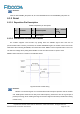
UART_RXD
Module_VDD
10K
4.7K
1nF
MCU_VDD
4.7K
1nF
10K
UART_TXD
UART_ TXD
UART_RXD
MODULE
DCE
MCU
DTE
MCU_VDD
Module_VDD
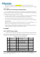
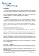
Figure6-10 Module and MCU UART Level Conversion Circuit
For more information on the application of UART serial port, please refer to “FIBOCOM UART
Application Design Instructions”.
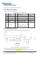
6.5 I2C
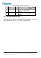
N510-GL provides a set of I2C interfaces, which are defined as follows:
Table6-9 I2C pin definition description
PIN
Pin Name
I/O
Pin Description
Power Domain
(TYP)
56
I2C_SCL
I/O
I2C Serial Clock Signal (The pin can
be suspended when not in use.)
2.8V
52
I2C_SDA
O
I2C Serial Port Data Signal(The pin
can be suspended when not in use.)
2.8V
Because the N510-GL module has pulled up the I2C signal to 2.8V through 4.7K resistance, it is
not necessary to pull up the I2C signal in the actual use process.
6.6 ADC
6.6.1 ADC Pin Description
The definition of ADC pin is as follows: