FIBOCOM SU806 Series Hardware Guide Version: V2.0.
Applicability Type NO Product Model 1 SU806-CN-00 2 SU806-CN-01 3 SU806-CN-11 4 SU806-CN-10 5 SU806-EAU-00 Description 8GB e.MMC+8Gb LPDDR3.SDRAM, 4G frequency, Android 10, applicable to China 8GB e.MMC+8Gb LPDDR3.SDRAM, 4G frequency diversity removal, Android 9, applicable to China 16GB e.MMC+16Gb LPDDR3.SDRAM, 4G frequency diversity removal, Android 9, applicable to China 16GB e.MMC+16Gb LPDDR3.SDRAM, 4G frequency, Android 10, applicable to China 8GB e.MMC+8Gb LPDDR3.
Copyright Copyright ©2021 Fibocom Wireless Inc. All rights reserved. Without the prior written permission of the copyright holder, any company or individual is prohibited to excerpt, copy any part of or the entire document, or transmit the document in any form. Notice The document is subject to update from time to time owing to the product version upgrade or other reasons. Unless otherwise specified, the document only serves as the user guide.
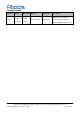
Change History Version V2.0.0 Author Reviewer Mo Xiaoke Tu Min He Sihai Li Xiyi Approver Update Date Description Initial version, modify pin Chen Guojiang 2021-02-01 function based on SU806 Series Hardware Guide v1.0.2 Reproduction forbidden without Fibocom Wireless Inc. written authorization - All Rights Reserved.
Contents 1 2 Introduction .................................................................................................................. 8 1.1 Instruction ..................................................................................................................... 8 1.2 Reference Standards .................................................................................................... 8 1.3 Related Document ..............................................................................
3.13 Charge Enable Interface ............................................................................................. 44 3.14 Vibration Motor Driver Interface .................................................................................. 44 3.15 LCM............................................................................................................................ 44 3.16 TP................................................................................................................
6.4 7 8 9 10 Bluetooth Performance ............................................................................................... 68 GNSS ............................................................................................................................69 7.1 Overview .................................................................................................................... 69 7.2 Performance ........................................................................................
1 Introduction 1.1 Instruction This document describes the electrical characteristics, RF performance, structure size, application environment, etc. of SU806 series module. With the assistance of the document and other instructions, the developers can quickly understand the hardware functions of the SU806 series module and develop products. 1.2 Reference Standards The design of product refers to the following standards: 3GPP TS 51.010-1 V10.5.
Bluetooth Radio Frequency TSS and TP Specification 1.2/2.0/2.0+EDR/2.1/2.1+EDR/3.0/3.0+HS, August 6, 2009 Bluetooth Low Energy RF PHY Test Specification, RF-PHY.TS/4.0.0, December 15, 2009 1.3 Related Document FIBOCOM Sx806 Series SMT Design Guide This equipment has been tested and found to comply with the limits for a Class B digital device, pursuant to part 15 of the FCC rules. These limits are designed to provide reasonable protection against harmful interference in a residential installation.
can use wording such as the following: “Contains FCC ID: ZMOSU806EAU” any similar wording that expresses the same meaning may be used. This equipment complies with FCC radiation exposure limits set forth for an uncontrolled environment. This equipment should be installed and operated with a minimum distance of 20cm between the radiator & your body. This transmitter must not be co-located or operating in conjunction with any other antenna or transmitter. The module is limited to OEM installation ONLY.
2 Product Overview 2.1 Product Introduction SU806 series smart module integrates core components such as Baseband, eMCP, PMU, Transceiver, PA; it supports long distance multi-mode communication such as FDD/TDD-LTE, WCDMA, GSM and WIFI/BT short-distance radio transmission technology, as well as GNSS wireless positioning technology. SU806 series module is embedded with Android operating system and support various interfaces such as MIPI/USB/UART/SPI/I2C.
2.2 Product Specification SU806 series module is available in 262 LCC+LGA package that includes 146 LCC pins and 116 LGA pins. The dimension is 40.5mm×40.5mm×2.8mm. It can be embedded in various M2M applications. It is suitable for the development of smart devices such as smart POS, cash registers, robots, UAVs, smart homes, security monitoring and multimedia terminals. Its detailed performance is shown in the following table. Table 2-3 Main performance Performance Description Power Supply DC:3.5~4.
Performance Description CAT14 HSDPA: Maximum downlink rate 21Mbps Support 3GPP R10 Support FDD/TDD CAT4 LTE features Support 1.4-20M RF bandwidth Downlink support 2 × 2 MIMO Maximum uplink rate 50Mbps, maximum downlink rate 150Mbps WLAN features Support 2.4G WLAN wireless communication, support 802.11b, 802.11g, 802.11n, the maximum rate up to 72.2Mbps Bluetooth BT4.
Performance Description One 4-line serial interface supporting RTS and CTS hardware flow control One 2-line serial interface (reserved) One 2 line debug serial interface SDIO interface I2C interface Support SD3.0, 4bit SDIO; SD card supports hot plug Multiple I2C interfaces, can be used for peripherals such as TP, camera, and sensor ADC interface One universal 12bits ADC RTC Support Antenna interface MAIN antenna, DRX antenna, GNSS antenna, WIFI/BT antenna Dimension: 40.5mm×40.5mm×2.
--Communication expansion interface (USB/UART/I2C/SDIO/SPI) --(U)SIM card interface --MIPI DSI interface --MIPI CSI Interface -- Analog audio interface ANT_MAIN TXM SAW SAW SAW LNA SAW DRx PRx LPDDR3 SDRAM eMMC Tx Power Transceiver PRx VBAT 26M XO VRTC ADC Switch Duplex PA AUDIO ANT_WIFI/BT ANT_GNSS ANT_DIV PMU Control Air RESET Interface Memory Baseband PWRKEY Multimedia LCM TP CAM Connectivity I2C SPI UART (U)SIM SDIO GPIO USB VoL key Figure 2-1 Functional block d
2.4 Pin Definition 2.4.1 Pin Assignment Figure 2-2 Pin assignment (top view) Note: “NC” represent No Connect, the pin of this position is reserved and does not need to be connected. Reproduction forbidden without Fibocom Wireless Inc. written authorization - All Rights Reserved.
2.4.
Pin Name Pin Number I/O Functional Description Note Power output for (U)SIM card 2 - VDDSIM2 21 PO VDDCAMA 129 PO VDDCAMCORE 151 PO Output for camera digital power - VDD2V8 228 PO 2.8V voltage output - VIB_DRV_N 28 PO Vibrator drive output Output for camera analog power, 2.
Pin Name Pin Number I/O Functional Description Note reset CBL_PWR_N Power on key 2, just have 261 DI UIM2_DATA 20 I/O (U)SIM card 2 data - UIM2_CLK 19 DO (U)SIM card 2 clock - UIM2_RST 18 DO (U)SIM card 2 reset - power on function Active low (U)SIM card interface UIM2_DET 17 DI (U)SIM card 2 hot plug detection Disabled by default, cannot used as general GPIO UIM1_DATA 25 I/O (U)SIM card 1 data - UIM1_CLK 24 DO (U)SIM card 1 clock - UIM1_RST 23 DO (U)SIM card 1 re
Pin Name Pin Number I/O Functional Description Note TP_I2C_SCL 47 DO I2C clock For touch panel by default TP_I2C_SDA 48 I/O I2C data For touch panel by default CAM_I2C_SCL0 83 DO I2C clock For rear camera by default CAM_I2C_SDA0 84 I/O I2C data For rear camera by default CAM_I2C_SCL1 239 DO I2C clock For front/depth camera by default CAM_I2C_SDA1 240 I/O I2C data For front/depth camera by default USB interface USB_VBUS 141,142 PI USB 5V input - USB_DP 14 AI/AO USB
Pin Name Pin Number I/O Functional Description Note SPI_MISO 118 DI SPI master input slave output - SPI_MOSI 119 DO SPI master output slave input - MIPI_DSI0_CLK_N 52 AO MIPI display serial interface - MIPI_DSI0_CLK_P 53 AO clock - MIPI_DSI0_LN0_N 54 AO - MIPI_DSI0_ LN0_P 55 AO - MIPI_DSI0_ LN1_N 56 AO - MIPI_DSI0_ LN1_P 57 AO MIPI display serial interface - MIPI_DSI0_LN2_N 58 AO lane - MIPI_DSI0_LN2_P 59 AO - MIPI_DSI0_LN3_N 60 AO - MIPI_DSI0_LN3_P 61
Pin Name Pin Number I/O Functional Description Note MIPI_CSI0_LN1_P 156 AI MIPI_CSI0_LN1_N 232 AI MIPI_CSI0_LN2_P 157 AI MIPI_CSI0_LN2_N 233 AI MIPI_CSI0_LN3_P 158 AI MIPI_CSI0_LN3_N 234 AI MCAM_MCLK 74 DO Rear camera master clock - MCAM_RST 79 DO Rear camera reset signal - MCAM_PWDN 80 DO Rear camera power down - MIPI_CSI1_CLK_N 63 AI MIPI front camera serial - MIPI_CSI1_CLK_P 64 AI interface clock - MIPI_CSI1_LN0_N 65 AI MIPI_CSI1_LN0_P 66 AI MIPI fron
Pin Name Pin Number I/O Functional Description Note Audio interface SPK_P 10 AO Speaker amp + output - SPK_M 11 AO Speaker amp - output - EAR_P 8 AO Earpiece PA + output - EAR_M 9 AO Earpiece PA - output - HPH_L 138 AO HPH_GND 137 - HPH_R 136 AO Headphone PA left channel output Headphone PA ground sensing Headphone PA right channel - output HPH_DET 139 AI Headset detection - MIC2_P 6 AI Headset MIC difference input + - MIC1_M 5 AI MIC1 difference input - -
Pin Name Pin I/O Functional Description Note 110 DI Accelerometer sensor interrupt - ADC 128 AI ADC detection - LED_B 194 AI RGB LED input2 - LED_G 195 AI RGB LED input1 - LED_R 196 AI RGB LED input0 - ACCL_INT Number Other interface The module does not support charging, and CHG_EN 210 AO Charge enable DC-DC circuit can be added if charging function is required.
Pin Name Pin Number I/O Functional Description Note GPIO_91 108 I/O INPUT(WPD) GPIO_32 112 I/O INPUT(WPD) GPIO_89 113 I/O OUTPUT GPIO_122 115 I/O WPD GPIO_139 123 I/O INPUT(WPU) GPIO_140 124 I/O INPUT(WPU) GPIO_88 153 I/O INPUT(WPU) GPIO_30 159 I/O INPUT(WPD) GPIO_29 183 I/O INPUT(WPD) GPIO_27 187 I/O INPUT(WPD) GPIO_85 202 I/O OUTPUT GPIO_154 203 I/O INPUT(WPD) GPIO_155 205 I/O INPUT(WPD) GPIO_28 206 I/O INPUT(WPD) INPUT(WPD) GPIO_24 207 I/O B
Pin Name Pin Number I/O Functional Description Note NC 接口 NC 154, 191, 197, 199, 204, 222 to 224, 247 to 249, 255 Keep floating Note: H: High-voltage tolerant L: Low-voltage tolerant Hiz: High impedance WPU: Weak pull up WPD: Weak pull down The GPIOs with “WPU” aren’t recommended as the enable control of default highly efficient devices. For example, backlight enable of LCM and audio amplifier enable. Reproduction forbidden without Fibocom Wireless Inc. written authorization - All Rights Reserved.
3 Application Interface 3.1 Power Supply The SU806 series module provides four VBAT pins for connecting to external power supply source. The input range of power is 3.5V to 4.2V and the recommended value is 3.8V. The performance of the power supply such as its load capacity, ripple etc. will directly affect the operating performance and stability of the module.
VBAT Module + 220uF 220uF 1uF 100nF 39pF 33pF 18pF 8.2pF 6.
VRTC input voltage - 3.0 - V VRTC input current - 40 - uA The reference design of VRTC pin powered by external power source is shown the following figure: Module VRTC + Coin cell Figure 3-3 VRTC reference design 3.1.3 Power Output The SU806 series module provides multiple power outputs for peripheral circuits. It is recommended to connect 33pF and 10pF capacitors in parallel with every power to avoid high frequency interference effectively.
VDDCAMCORE 1.00625-1.4 1.2 400 VDD2V8 1.8-3.3 2.8 200 VIB_DRV_N 1.8-3.3 3.3 100 3.2 Control Signal 3.2.1 Power on/off SU806 series module provides one-way power on/off control signal to module’s power on/off, restart and sleep/wake up. Its pin definition is shown as follow table: Table 3-5 Power on/off signal Pin Name Pin I/O Description Note Active low, module power on/off, restart, - Number KEY_PWR_ON 114 DI CBL_PWR_N 261 DI 3.2.1.
KEY_PWR_ON 3s≤t≤6s 100pF 10K 47K Figure 3-5 OC drive power on reference design The power on timing is shown as follows: VBAT 3.5s≤t≤6s KEY_PWR_ON VDD1V85 Other Powers Figure 3-6 Power on timing 3.2.1.2 Power off Normal power off: when module in operating mode, pull down KEY_PWR_ON pin 0.6s~6s, user interface will display selection box (select power off or restart).
enter sleep mode. When module in sleep mode, pull down KEY_PWR_ON pin 0.1s~0.5s and then release it, module can be waked up. 3.2.2 Reset Support one key (KEY_PWR_ON) reset and two key (KEY_PWR_ON & KEY_RESIN_N) reset; and two key reset mode is default. One key (KEY_PWR_ON) reset: when module in operating mode, pull down KEY_PWR_ON pin 0.6s~6s, user interface will display selection box (select power off or restart); pull down KEY_PWR_ON pin 7s~10s module will be forced reset.
Table 3-6 USB2.0 pin definition Pin Pin Name Number I/O Description Note USB_VBUS 141,142 PI USB VBUS 5V input - USB_DP 14 AI/AO USB HS data + - USB_DM 13 AI/AO USB HS data - - USB_ID 16 DI USB OTG detection - The reference design of USB2.0 is show as follow figure: Connector Module VBUS USB_DM DM USB_DP DP USB_ID ID 1uF USB_VBUS GND Figure 3-8 USB2.0 reference design Reproduction forbidden without Fibocom Wireless Inc. written authorization - All Rights Reserved.
Module GPIO Connector DC-DC VBAT VBUS USB_DM DM USB_DP DP USB_ID ID 1uF USB_VBUS GND Figure 3-9 USB2.0 reference design (with OTG function) Note: 1) Please choose junction capacitor less than 1pF for ESD protection device of USB_DP/DM 2) USB_DP and USB_DM are high-speed differential signal. The highest transmission rate is 480Mbps.
3.4 UART SU806 series module defines three UART ports,all are 1.8V voltage domain ,the function of UART2 has not achieve at present.
Level Shifter VDD_1V8 VCCA VCCB 0.1uF 0.1uF VDD_MCU OE GND UART_TXD A1 B1 MCU_TXD UART_RXD A2 B2 MCU_RXD UART_CTS A3 B3 MCU_CTS A4 B4 UART_RTS MCU_RTS Figure 3-10 Level shift reference design The other level translator circuit is shown as Figure 3-11, The rest input and output circuit design of dotted line please refer to solid line part, but pay attention to signal connection direction. Figure 3-11 Level shift reference design 2 3.
SPI_CS 117 DO SPI chip selects - SPI_MISO 118 DI SPI master input slave output - SPI_MOSI 119 DO SPI master output slave input - 3.6 (U)SIM The SU806 series module supports two (U)SIM cards, dual-SIM dual-standby single-active (default double) and both support hot plug (default off).
VDD1V85 Connector 100K Module UIM_VDD VCC 10K 22R UIM_DATA DATA 22R DET UIM_DETECT 22R CLK UIM_CLK 22R UIM_RST 2.2uF RST 18pF ESD Figure 3-12 (U)SIM reference design (U)SIM card design notice: 1) The length from the (U)SIM card holder to module should less than 100mm. 2) The layout and routing of the (U)SIM card must be kept away from EMI interference sources such as RF antenna and digital switch power.
Pin Pin Name Number I/O Description Note SD_CLK 39 DO SD card clock - VDDSDCORE 38 PO Power for SD card - VDDSDIO 32 PO Power for SDIO interface - SDIO interface reference design is show in the following figure: VDDSDCORE VDD1V85 100MHz_120R 100nF 4.
Interrupt Pin Name Pin Number H/L/Hiz After Reset After Reset GPIO_134 33 L INPUT(WPD) YES GPIO_129 90 L INPUT(WPD) YES GPIO_135 98 H INPUT(WPU) YES GPIO_136 99 H INPUT(WPU) YES GPIO_137 100 H INPUT(WPU) YES GPIO_131 101 L INPUT(WPD) YES GPIO_130 102 L INPUT(WPD) YES GPIO_133 103 L INPUT(WPD) YES GPIO_132 104 L INPUT(WPD) YES GPIO_121 105 L OUTPUT YES GPIO_138 106 H INPUT(WPU) YES GPIO_91 108 L INPUT(WPD) YES GPIO_32 112 L INPUT(WPD) YES
Interrupt Pin Name Pin Number H/L/Hiz After Reset After Reset GPIO_24 207 L INPUT(WPD) YES GPIO_11 241 L INPUT(WPD) YES GPIO_7 242 L INPUT(WPD) YES GPIO_143 243 H INPUT(WPU) YES GPIO_10 244 L INPUT(WPD) YES GPIO_141 97 H INPUT(WPU) YES GPIO_26 252 L INPUT(WPD) YES GPIO_22 253 L INPUT(WPD) YES GPIO_23 254 L INPUT(WPD) YES Function Note: H: High-voltage tolerant L: Low-voltage tolerant Hiz: High impedance WPU: Weak pull up WPD: Weak pull down 3.
CAM_I2C_SCL0 83 DO I2C clock For rear/front camera by default CAM_I2C_SDA0 84 I/O I2C data For rear/front camera by default CAM_I2C_SCL1 239 DO I2C clock For depth camera by default CAM_I2C_SDA1 240 I/O I2C data For depth camera by default Note: When I2C has more than one peripheral, please ensure the uniqueness of every peripheral address. 3.
3.12 Battery Power Supply Interface SU806 series module just support circuit modes coulomb counter fuel gauge, if use coulomb counter IC externally, please connect SENSE_P and SENSE_N pin to GND.
3.13 Charge Enable Interface Table 3-17 Charge enable interface pin definition Pin Name Pin I/O Number Description Note The module does not support CHG_EN 210 AO Charge enable output charging, and DC-DC circuit can be added if charging function is required. 3.
Pin Pin Name Number I/O Description Note MIPI_DSI0_LN1_P 57 AO MIPI display serial interface Lane 1+ - MIPI_DSI0_LN2_N 58 AO MIPI display serial interface Lane 2- - MIPI_DSI0_LN2_P 59 AO MIPI display serial interface Lane 2+ - MIPI_DSI0_LN3_N 60 AO MIPI display serial interface Lane 3 - - MIPI_DSI0_LN3_P 61 AO MIPI display serial interface Lane 3 + - LCD_RST 49 DO LCD reset - PWM 29 DO LCD backlight PWM - LCD_TE 50 DI LCD tearing effect GPIO_25 190 DO Keep flo
LCM design notice: 1) MIPI is a high-speed signal. It is recommended to connect the common mode inductor in series near the LCD connector to reduce the electromagnetic interference of the circuit. 2) MIPI routing is recommended to be in the inner layer, with three-dimensional grounding; 3) The MIPI signal needs to be controlled with a differential impedance of 100Ω tolerance ±10%; 4) The total length of the trace must ≤70mm, VIAs≤4; 5) The intra lane match of MIPI differential pair signal must ≤ 0.
power, interrupt, reset pins.
Pin Pin Name Number I/O 4-Lane+2-Lane+1-Lane Note VDD1V8 125 PO DOVDD power supply, 1.8V VDDCAMA 129 PO AVDD power supply, 2.8V VDDCAMMOT 152 PO VDDCAMCORE 151 PO DVDD power supply, 1.
Pin Pin Name Number I/O 4-Lane+2-Lane+1-Lane Note MIPI_CSI1_LN0_P 66 AI MIPI front camera serial interface lane 0 - - MIPI_CSI1_LN1_N 67 AI MIPI front camera serial interface lane 1 + - MIPI_CSI1_LN1_P 68 AI MIPI front camera serial interface lane 1 - - SCAM_MCLK 75 DO Front camera master clock - SCAM_RST 81 DO Front camera reset - SCAM_PWDN 82 DO Front camera power down - MIPI_CSI1_LN3_N 70 AI MIPI depth camera serial interface clock - - MIPI_CSI1_LN3_P 71 AI MIP
VCCCAMMOT VDDCAMA VDD1V8 VDDCAMCORE VDD1V85 DOVDD NC NC DVDD Module AFVDD AVDD MCAM_PWDN PWD MCAM_RST RST CAM_I2C_SCL0 SCL CAM_I2C_SDA0 SDA MIPI_CSI0_CLK_P CLK_P EMI MIPI_CSI0_CLK_N CLK_N DAT3_P MIPI_CSI0_LN3_P EMI MIPI_CSI0_LN3_N DAT3_N DAT2_P MIPI_CSI0_LN2_P EMI MIPI_CSI0_LN2_N DAT2_N DAT1_P MIPI_CSI0_LN1_P EMI MIPI_CSI0_LN1_N MIPI_CSI0_LN0_P CAM Connector CAM Connector MCLK MCAM_MCLK DAT1_N DAT0_P EMI DAT0_N 1uF 100nF 10uF 100nF 1uF 10uF MIPI_CSI0_LN0_N Figu
3.17.3 Depth Camera Pin definition of depth camera is shown as follow: VDD1V8 VDDCAMA VDD1V85 AVDD MCLK DCAM_MCLK DCAM_PWDN PWD DCAM_RST RST CAM_I2C_SCL1 SCL CAM_I2C_SDA1 SDA MIPI_CSI1_LN3_P EMI MIPI_CSI1_LN3_N CLK_P CAM Connector 100nF NC NC Module 10uF 1uF DOVDD CLK_N DAT0_P MIPI_CSI1_LN2_P EMI MIPI_CSI1_LN2_N DAT0_N Figure 3-19 Depth camera reference design 3.17.
11) The analog voltage VDDCAMA routing should be away from interference sources, otherwise it is easy to bring interference of power noise; 12) Camera analog power supply suggest to add LDO with high PSRR ability and place it near camera. Table 3-23 Length of MIPI_CSI differential signal in module Pin Pin Name Number Length (mm) MIPI_CSI0_CLK_P 229 24.6976 MIPI_CSI0_CLK_N 230 24.4567 MIPI_CSI0_LN0_P 155 24.59549 MIPI_CSI0_LN0_N 231 24.50157 MIPI_CSI0_LN1_P 156 24.
3.18 Sensor SU806 series module supports I2C interface to communicate with various types of sensors, such as accelerometer sensor, ambient light sensor and magnetic sensor etc.
Pin Pin Name Number I/O Description Note MIC2_P 6 AI Headset mic input - MIC1_M 5 AI Main mic difference input- - MIC1_P 4 AI Main mic difference input+ - MIC3_P 220 AI Sub-mic input - Design notice: 1) SU806 series module has MIC bias circuit internally, and no external addition is required. 2) The SPK is configured as class D amplifier output, cannot connect with amplifier externally, it is recommended to connect 8Ω speakers.
3.19.2 Microphone Circuit Design Module 100pF MIC_P 33pF 33pF MIC_M Figure 3-20 Microphone reference design 3.19.3 Earpiece Circuit Design Module 0R 100pF EAR_P 0R 33pF 33pF EAR_M Figure 3-21 Earpiece reference design Reproduction forbidden without Fibocom Wireless Inc. written authorization - All Rights Reserved.
3.19.4 Headset Circuit Design Module 33pF MIC2_P HPH_L HPH_R 1K HPH_DET 0R 33pF 33pF HPH_GND Figure 3-22 Headset reference design Note: Please choose bidirectional TVS for headset ESD protection. 3.19.5 Speaker Circuit Design Module SPK_P 39pF 39pF SPK_M Figure 3-23 Speaker reference design Reproduction forbidden without Fibocom Wireless Inc. written authorization - All Rights Reserved.
3.20 Force Download Interface SU806 series module provides KEY_FORCE_BOOT pin as an emergency download interface. Connect the KEY_FORCE_BOOT with GND when power on, the module can enter the emergency download mode which is used for the final processing mode when the product fails to power on or run normally. To facilitate the subsequent software upgrade and product debugging, please reserve the test pin of this pin.
4 Antenna Interface SU806 series module support 2/3/4G main antenna/diversity reception antenna, WIFI/BT antenna and GNSS antenna. 4.1 MAIN/DRX Antenna SU806 series module provides two 2G/3G/4G antenna interfaces. The ANT_MIAN is used to receive and transmit RF signal, the ANT_DRX is used for diversity reception. Table 4-1 Main/DRX pin definition Pin Name Pin Number I/O Description Note ANT_MAIN 87 AI/AO 2G/3G/4G main antenna - ANT_DRX 131 AI Diversity reception antenna - 4.1.
Mode Band Tx (MHz) Rx (MHz) Band 40 2300-2400 2300-2400 Band 41 2535-2675 2535-2675 Band Tx (MHz) Rx (MHz) 850 824-849 869-894 900 880-915 925-960 1800 1710-1785 1805-1880 1900 1850-1910 1930-1990 Band 1 1920-1980 2110-2170 Band 2 1850-1910 1930-1990 Band 5 824-849 869-894 Band 8 880-915 925-960 Band 1 1920-1980 2110-2170 Band 3 1710-1785 1805-1880 Band 5 824-849 869-894 Band 7 2500-2570 2620-2690 Band 8 880-915 925-960 Band 20 791-821 832-862 Band 28
4.1.2 Antenna Reference Design When use the SU806 series module, it is necessary to connect the antenna pin with the RF connector or antenna feed point on the main board via an RF trace. Microstrip trace is recommended for RF trace, with insertion loss within 0.2dB and impedance at 50Ω.A π-type circuit is reserved between the module and the antenna connector (or feed point) for antenna debugging.
4.2.2 WIFI/BT Antenna Reference Design WIFI/BT antenna reference design is shown in the following figure: WIFI/BT_Antenna 0R ANT_WIFI/BT NC NC Figure 4-2 WIFI/BT antenna reference design 4.3 GNSS Antenna GNSS supports GPS/BeiDou. Table 4-6 GNSS antenna interface definition Pin Name Pin Number I/O Description Note ANT_GNSS 121 AI GNSS antenna - 4.3.1 Operating Frequency Table 4-7 GNSS operating frequency Mode Frequency Unit GPS 1575.42±1.023 MHz BeiDou 1561.098±2.046 MHz 4.3.
The GNSS antenna reference design is shown in the following figure: Module GNSS_Antenna 0R ANT_GNSS NC 82nH Figure 4-3 GNSS passive antenna reference design Note: For GNSS passive antenna, it is recommended to add an 82nH indictor near antenna connector to improve GNSS antenna’s ability of resist ESD. For better ability of resist ESD, please choose TVS that junction capacitance less than 0.5pF, recommended type: ESD9D5U, with 0.5pF junction capacitance and 5.0V embedded voltage. 4.3.2.
VDD_3.3V GNSS_Antenna 0R 100pF 1uF Module 33pF 10R 56nH ANT_GNSS NC NC Figure 4-4 GNSS active antenna reference design 4.4 Antenna Requirement SU806 series module provides four antenna interfaces: main, diversity, WIFI/BT and GNSS.
SU806 Series Module Antenna Requirement Standard Antenna Requirement Frequency range: 1559MHz~1607MHz Polarization type: right-circular or linear polarization VSWR: < 2 (typical) GNSS Passive antenna gain: > 0dBi Active antenna NF: < 15dB (typical) Active antenna gain: > -2dBi Reproduction forbidden without Fibocom Wireless Inc. written authorization - All Rights Reserved.
5 RF PCB Layout Design Guide For user PCB, the characteristic impedance of all RF signal traces should be within 50Ω. In general, the impedance of the RF signal trace is determined by the dielectric constant of the material, the trace width (W), the ground clearance (S) and the height of the reference ground plane (H). The control of the characteristic impedance of the PCB usually in two ways: microstrip trace and coplanar waveguide.
Figure 5-3 Four-layer PCB coplanar waveguide structure (reference ground layer3) Figure 5-4 Four-layer PCB coplanar waveguide structure (reference ground layer4) In the design of RF antenna interface circuit, in order to ensure good performance and reliability of the RF signal, it is recommended to observe the following principles: The impedance simulation tool should be used to accurately control the RF signal cable at 50Ω impedance.
6 WIFI and Bluetooth 6.1 WIFI Overview SU806 series module supports 2.4G WLAN wireless communications and 802.11b, 802.11g, 802.11n standards, with a maximum speed up to 72.2Mbps. Its characteristics are as follows: Support Wake-on-WLAN (WoWLAN) Support ad hoc mode Support WAPI Support AP mode Support Wi-Fi Direct Support MCS 0-7 for HT20 6.2 WIFI Performance Test condition:3.
Frequency Mode Date Rate Bandwidth (MHz) Sensitivity (dBm) MCS0 20 -85 MCS7 20 -70 802.11n 6.3 Bluetooth Overview SU806 series module supports BT4.2 (BR/EDR+BLE) standards. The modulation method supports GFSK, 8-DPSK and π/4-DQPSK.BR/EDR. Channel bandwidth is 1MHz and can accommodate 79 channels. The BLE channel bandwidth is 2MHz and can accommodate 40 channels. Its main features are as follows: BT 4.
7 GNSS 7.1 Overview SU806 series smart module supports GPS/BeiDou positioning systems. The module is embedded with LNA which can effectively improve the sensitivity of GNSS. 7.2 Performance Test condition:3.8V power supply, environment temperature 25°C Table 7-1 GNSS positioning performance Parameter Description Typical Result Unit Acquisition -146 dBm Tracking -155 dBm -130dBm 39.
8 Electrical, Reliability and RF Performance 8.1 Recommended Parameters Table 8-1 Recommended parameters Parameter Min Normal Max Unit VBAT 3.5 3.8 4.2 V USB_VBUS 4.75 5 5.25 V VRTC - 3.0 3.35 V Operating Temperature -20 25 65 ℃ Storage Temperature -40 25 95 ℃ 8.2 Absolute Maximum Ratings The functionality of SU806 series module is subject to the absolute maximum/minimum values listed in the following table. Do not exceed these parameters or the part may be damaged permanently.
Parameter Description Software power off current Isleep IGSM-RMS IGSM-MAX IGPRS-RMS IEGPRS-RMS IWCDMA-RMS Condition By AT command or select the power off menu in LCM selection box Typical Result Unit TBD GSM MFRMS=5 TBD WCDMA DRX=8 TBD TDD LTE DPC (Default Paging Cycle)=#256 TBD FDD LTE DPC (Default Paging Cycle)=#256 TBD Radio Off AT+CFUN=4 Flight Mode TBD EGSM900@ PCL=5 TBD GSM voice EGSM900@ PCL=19 TBD RMS Current DCS1800@ PCL=0 TBD DCS1800@ PCL=15 TBD GSM voice EGS
Parameter Description Condition Typical Result Band1@ max power(10MHz,1RB) TBD FDD data Band3@ max power(10MHz,1RB) TBD RMS Current Band5@ max power(10MHz,1RB) TBD Band8@ max power(10MHz,1RB) TBD Band34@ max power(10MHz,1RB) TBD Band38@ max power(10MHz,1RB) TBD Band39@ max power(10MHz,1RB) TBD Band40@ max power(10MHz,1RB) TBD Band41@ max power(10MHz,1RB) TBD ILTE-RMS TDD data RMS Current Unit mA Table 8-4 SU806-CN-01/SU806-CN-11 power consumption Parameter Description Condition
Parameter IGPRS-RMS IEGPRS-RMS IWCDMA-RMS Typical Description Condition Peak current DCS1800@ PCL=0 1300 EGSM900@ Gamma=3 (1UL/4DL) 223 GPRS data EGSM900@ Gamma=3 (4UL/1DL) 494 RMS Current DCS1800@ Gamma=3 (1UL/4DL) 179 DCS1800@ Gamma=3 (4UL/1DL) 339 EGSM900@ Gamma=6 (1UL/4DL) 169 EGPRS data EGSM900@ Gamma=6 (4UL/1DL) 498 RMS Current DCS1800@ Gamma=5 (1UL/4DL) 161 DCS1800@ Gamma=5 (4UL/1DL) 468 WCDMA Band1@ max power 589 RMS Current Band8@ max power 598 Band1@ max power (
Parameter Isleep IGSM-RMS IGSM-MAX IGPRS-RMS IEGPRS-RMS IWCDMA-RMS ILTE-RMS Typical Description Condition GSM MFRMS=5 3.1 WCDMA DRX=8 3.15 TDD LTE DPC (Default Paging Cycle)=#256 2.8 FDD LTE DPC (Default Paging Cycle)=#256 2.8 Radio Off AT+CFUN=4 Flight Mode 2.
Parameter Typical Description Condition RMS Current Band3@ max power (10MHz,1RB) 625 Band5@ max power (10MHz,1RB) 580 Band8@ max power (10MHz,1RB) 618 Band34@ max power (10MHz,1RB) 336 Band38@ max power (10MHz,1RB) 326 Band39@ max power (10MHz,1RB) 322 Band40@ max power (10MHz,1RB) 342 Band41@ max power (10MHz,1RB) 354 TDD data RMS Current Result Unit Table 8-6 Power consumption of SU806-EAU-00 Parameter Description Condition Static leakage current Power supply, not power on Iof
Parameter IGSM-MAX IGPRS-RMS IEGPRS-RMS Description Condition Typical Result DCS1800@ PCL=0 TBD DCS1800@ PCL=15 TBD PCS1900@ PCL=0 TBD PCS1900@ PCL=15 TBD GSM850@ PCL=5 TBD GSM voice EGSM900@ PCL=5 TBD Peak current DCS1800@ PCL=0 TBD PCS1900@ PCL=0 TBD GSM850@ Gamma=3 (1UL/4DL) TBD GSM850@ Gamma=3 (4UL/1DL) TBD EGSM900@ Gamma=3 (1UL/4DL) TBD GPRS data EGSM900@ Gamma=3 (4UL/1DL) TBD RMS current DCS1800@ Gamma=3 (1UL/4DL) TBD DCS1800@ Gamma=3 (4UL/1DL) TBD PCS1900@ Gamma
Parameter IWCDMA-RMS Description Typical Condition Result PCS1900@ Gamma=5 (1UL/4DL) TBD PCS1900@ Gamma=5 (4UL/1DL) TBD Band1@ max power TBD WCDMA Band2@ max power TBD RMS current Band5@ max power TBD Band8@ max power TBD Band1@ max power (10MHz,1RB) TBD Band3@ max power (10MHz,1RB) TBD Band5@ max power (10MHz,1RB) TBD Band7@ max power (10MHz,1RB) TBD Band8@ max power (10MHz,1RB) TBD Band20@ max power (10MHz,1RB) TBD Band28@ max power (10MHz,1RB) TBD Band38@ max power (10MH
Mode Band Max Power (dBm) Min Power (dBm) 900 (8PSK) 27.0±3 5±5 1800 (8PSK) 26.0±3 0±5 Band 1 24+1/-3 < -49 Band 8 24+1/-3 < -49 Band 1 23.0±2 < -39 Band 3 23.0±2 < -39 Band 5 23.0±2 < -39 Band 8 23.0±2 < -39 Band 34 23.0±2 < -39 Band 38 23.0±2 < -39 Band 39 23.0±2 < -39 Band 40 23.0±2 < -39 Band 41 23.
Mode LTE FDD LTE TDD Band Max Power (dBm) Min Power (dBm) Band 5 24+1/-3 < -49 Band 8 24+1/-3 < -49 Band 1 23.0±2 < -39 Band 3 23.0±2 < -39 Band 5 23.0±2 < -39 Band 7 23.0±2 < -39 Band 8 23.0±2 < -39 Band 20 23.0±2 < -39 Band 28 23.0±2 < -39 Band 38 23.0±2 < -39 Band 40 23.0±2 < -39 Band 41 23.0±2 < -39 8.5 RF Receiver Sensitivity The sensitivity of each frequency band of the SU806 series module is shown in the following table: Test condition:3.
LTE TDD Band 34 TBD TBD TBD -96.3 dBm Band 38 TBD TBD TBD -96.3 dBm Band 39 TBD TBD TBD -96.3 dBm Band 40 TBD TBD TBD -96.3 dBm Band 41 TBD TBD TBD -94.3 dBm Table 8-10 RF receiver sensitivity of SU806-CN-01/SU806-CN-11 Mode 3GPP Band Primary Diversity PRX+Div Unit 900 -109 - - -102 dBm 1800 -108.8 - - -102 dBm Band 1 -110 - - -106.7 dBm Band 8 -110.5 - - -103.7 dBm Band 1 -98.8 - - -96.3 dBm Band 3 -98.4 - - -93.3 dBm Band 5 -98.
1800 -108.8 - - -102 dBm Band 1 -110 - - -106.7 dBm Band 8 -110.5 - - -103.7 dBm Band 1 -98.8 -99 -102 -96.3 dBm Band 3 -98.4 -98 -101.2 -93.3 dBm Band 5 -98.8 -99.5 -102.3 -94.3 dBm Band 8 -99.4 -99.2 -102.1 -93.3 dBm Band 34 -97.2 -97.3 -100.4 -96.3 dBm Band 38 -96.5 -96.8 -99.6 -96.3 dBm Band 39 -97 -97.5 -100.5 -96.3 dBm Band 40 -96.3 -97 -100 -96.3 dBm Band 41 -95.8 -96.5 -99.2 -94.
LTE TDD Band 5 TBD TBD TBD -94.3 dBm Band 7 TBD TBD TBD -94.3 dBm Band 8 TBD TBD TBD -93.3 dBm Band 20 TBD TBD TBD -93.3 dBm Band 28 TBD TBD TBD -94.8 dBm Band 38 TBD TBD TBD -96.3 dBm Band 40 TBD TBD TBD -96.3 dBm Band 41 TBD TBD TBD -94.3 dBm 8.6 Electrostatic Protection In the application of the module, due to static electricity generated by human body and charged friction between micro-electronics, etc.
9 Structural Specification 9.1 Product Appearance SU806 series module product appearance is shown in the following figure: Figure 9-1 Module product appearance 9.2 Structural Dimension The structural dimension of SU806 series module is shown in the following figure: Figure 9-2 Structural dimension Reproduction forbidden without Fibocom Wireless Inc. written authorization - All Rights Reserved.
9.3 PCB Soldering Pad and Stencil Design PCB soldering pad and stencil design please refer to FIBOCOM Sx806 Series SMT Design Guide. Reproduction forbidden without Fibocom Wireless Inc. written authorization - All Rights Reserved.
10 Production and Storage 10.1 SMT SMT production process parameters and related requirements please refer to FIBOCOM Sx806 Series SMT Design Guide. 10.2 Carrier and Storage Carrier and storage please refer to FIBOCOM Sx806 Series SMT Design Guide. Reproduction forbidden without Fibocom Wireless Inc. written authorization - All Rights Reserved.
Appendix A Terms and Acronyms Table A-0-1 Terms and acronyms Term Definition AMR Adaptive Multi-rate bps Bits Per Second CS Coding Scheme DRX Discontinuous Reception EGSM Extended GSM900 Band FDD Frequency Division Duplexing GMSK Gaussian Minimum Shift Keying GSM Global System for Mobile Communications HSDPA High Speed Down Link Packet Access IMEI International Mobile Equipment Identity Imax Maximum Load Current LED Light Emitting Diode LSB Least Significant Bit LTE Long Term Ev
Term Definition PCB Printed Circuit Board PDU Protocol Data Unit PSK Phase Shift Keying QAM Quadrature Amplitude Modulation QPSK Quadrature Phase Shift Keying RF Radio Frequency RHCP Right Hand Circularly PolarizedRMS RMS Root Mean Square RTC Real Time Clock Rx Receive SMS Short Message Service TDMA Time Division Multiple Access TE Terminal Equipment TX Transmitting Direction TDD Time Division Duplexing UART Universal Asynchronous Receiver & Transmitter UMTS Universal Mobi
Term Definition VIHmax Maximum Input High Level Voltage Value VIHmin Minimum Input High Level Voltage Value VILmax Maximum Input Low Level Voltage Value VILmin Minimum Input Low Level Voltage Value VImax Absolute Maximum Input Voltage Value VImin Absolute Minimum Input Voltage Value VOHmax Maximum Output High Level Voltage Value VOHmin Minimum Output High Level Voltage Value VOLmax Maximum Output Low Level Voltage Value VOLmin Minimum Output Low Level Voltage Value VSWR Voltage Standi
Appendix B GPRS Encoding Scheme Table B-0-1 GPRS encoding scheme Encoding method CS-1 CS-2 CS-3 CS-4 Rate 1/2 2/3 3/4 1 USF 3 3 3 3 Pre-coded USF 3 6 6 12 Radio Block excl.USF and BCS 181 268 312 428 BCS 40 16 16 16 Tail 4 4 4 - Coded Bits 456 588 676 456 Punctured Bits 0 132 220 - Data Rate Kb/s 9.05 13.4 15.6 21.4 Reproduction forbidden without Fibocom Wireless Inc. written authorization - All Rights Reserved.
Appendix C GPRS Multislot In the GPRS standard, 29 types of GPRS multislot modes are defined and can be used by mobile stations. The multislot class defines the maximum rate of uplink and downlink. The expression is 3+1 or 2+2, the first number represents the number of downlink timeslots and the second number represents the number of uplink timeslots. Active timeslot represents the total number of timeslots that the GPRS device can use for both uplink and downlink communications.
Appendix D EDGE Modulation and Encoding Method Table D-0-1 EDGE modulation and encoding method Coding Scheme Modulation Coding Family 1 Timeslot 2 Timeslot 4 Timeslot CS-1 GMSK - 9.05kbps 18.1kbps 36.2kbps CS-2 GMSK - 13.4kbps 26.8kbps 53.6kbps CS-3 GMSK - 15.6kbps 31.2kbps 62.4kbps CS-4 GMSK - 21.4kbps 42.8kbps 85.6kbps MCS-1 GMSK C 8.80kbps 17.6kbps 35.2kbps MCS-2 GMSK B 11.2kbps 22.4kbps 44.8kbps MCS-3 GMSK A 14.8kbps 29.6kbps 59.2kbps MCS-4 GMSK C 17.