FIBOCOM EVK-SC800 User Guide Version: V1.0.
Applicability Type No. Model Note 1 EVK-SC800-CN-00 NA Reproduction forbidden without Fibocom Wireless Inc. written authorization - All Rights Reserved.
Copyright Copyright©2020 Fibocom Wireless Inc. All rights reserved. Without the prior written permission of the copyright holder, any company or individual is prohibited to excerpt, copy any part of or the entire document, or distribute the document in any form. Notice The document is subject to update from time to time owing to the product version upgrade or other reasons. Unless otherwise specified, the document only serves as the user guide.
Content 1 Foreword ........................................................................................................................6 2 Product Overview ..........................................................................................................7 Product Introduction...................................................................................................... 7 Product Specifications .............................................................................................
No Response After Pressing the Power Button ........................................................... 39 No Output on Screen .................................................................................................. 39 DC Power Overcurrent Protection Is Caused by the High Current at the Startup ........ 39 Reproduction forbidden without Fibocom Wireless Inc. written authorization - All Rights Reserved.
1 Foreword This document describes the product introduction and instructions of the development suite EVK-SC800. With assistance of this document, application developers can quickly become familiar with and use EVKSC800. Reproduction forbidden without Fibocom Wireless Inc. written authorization - All Rights Reserved.
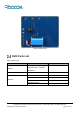
2 Product Overview Product Introduction Fibocom EVK-SC800 development board integrates a rich set of external interfaces. Cooperate with Fibocom SC80X, SQ808X, SU80X series of intelligent modules (see the ADP support list for details), it can provide a complete development and debugging platform for application developers to develop, verify, and demonstrate products quickly. Product Specifications Figure 2-1 Board interfaces Table 2-1 Product specifications Product Specification Voltage range:3.5-4.
Product Specification features Battery interface:3.7V lithium battery interface 4400mAh builtin 10K NTC resistance Camera Rear camera 5M 2lane MIPI CSI interface (with flash) Front camera 2M 1lane MIPI CSI interface Screen 5.5 inch 720P resolution 4 MIPI DSI interface LCD screen TP Capacitive touch screen interface Audio input: MIC1 (main MIC) MIC2 Audio Audio output: receiver, speaker (8Ω 1.2W), and headphone jack (MIC is supported) 2 USB2.0 TYPE_A_HOST interface USB 1 USB2.
Product Specification Storage temperature Structural characteristics Dimension -45℃ to 90℃(Non-battery power) 180mm×210mm Product Appearance Figure 2-2 Front view Reproduction forbidden without Fibocom Wireless Inc. written authorization - All Rights Reserved.
Figure 2-3 Rear view EVK Parts List Table 2-2 Parts list Name Specification 3.7V lithium battery interface Quantity Battery 4400mAh built-in 10K NTC 1 resistance USB cable Antenna Micro USB cable 1 MAIN antenna 1 DRX antenna 1 GNSS antenna 1 WIFI/BT antenna 1 Reproduction forbidden without Fibocom Wireless Inc. written authorization - All Rights Reserved.
ADP Support List Table 2-3 ADP support list Platform MSM8909 QCM2150 SL8541E Model ADP-SC800 series Note NA ADP-SC802 series NA ADP-SC806 series NA ADP-SC808 series NA ADP-SQ806 series NA ADP-SQ808 series NA ADP-SU806 series NA ADP-SU808 series NA Reproduction forbidden without Fibocom Wireless Inc. written authorization - All Rights Reserved.
3 Interface Specifications Power Interfaces EVK-SC800 supports two power supply modes: power supply interface (H10, H9) and battery supply interface (CON14). H10 + DC power H10 - VBAT GND TP_RST + BatteryTP_INT - Module Figure 3-1 Power supply mode 3.1.1 DC Interface When EVK-SC800 is powered by DC power supply, the positive terminal of the power supply is connected to BAT+ (H10), while the negative terminal of the power supply is connected to BAT- (H9). Power supply voltage ranges from 3.5V to 4.
Figure 3-2 DC interface 3.1.2 Battery Interface When EVK-SC800 is powered by battery, the battery should be inserted into the battery connector (CON14). The battery interface is shown as follows: Figure 3-2 Battery interface Table 3-1 Battery interface (CON14) Pin 1 Description VBAT Note VBAT 2 VBAT VBAT 3 VBAT_CON_TEMP Battery temperature detection pin 4 GND GND 5 GND GND Reproduction forbidden without Fibocom Wireless Inc. written authorization - All Rights Reserved.
Battery EVK-SC800 is equipped with a 4400 mAh(The actual capacity is subject to the actual goods received) lithium battery with built-in 10 K NTC resistance, which is composed of two 3.7 to 4.2V lithium batteries in parallel. The double-sided adhesive is stuck on the back of the development board near the battery interface. Please disconnect the DC power supply when using it, and then insert the battery into the battery connector (CON14). After the battery is used up, it should be charged in time.
The duration of each ADP button and the function of each ADP button shall be determined by consulting the specific module manual. ON/OFF button: the product can be started, shut down, slept and waked up by this button. - Press 2 seconds under shutdown state to boot the module. - Press 0.1 to 0.5 seconds to wake up the module after starting the sleep state. - After the module is started and waked up, press 0.1 to 0.5 seconds, and the module will enter sleep mode.
VDD1V85 100nF 100nF 2.
Figure 3-7 TP Interfaces VDD2V8 VDD1V85 10K 2.2K TP 2.2K Module VDD TS_I2C_SCL SCL TS_I2C_SDA SDA RESET TP_RST TP_INT INT 2.2uF 100nF Figure 3-8 TP Reference circuit Table 3-3 TP interfaces (CON4) Pin Description Note 1 GND GND 2 GND GND 3 GND GND 4 VDD_2V85_L17 TP power 2.85V 5 TP_RST_N TP reset 6 I2C_SCL_TP TP I2C clock 7 I2C_SDA_TP TP I2C data 8 TP_INT TP interrupt 9 GND GND 10 GND GND Reproduction forbidden without Fibocom Wireless Inc.
Camera The EVK-SC800 uses a dual camera based on the MIPI_CSI standard. The main camera is a 5 megapixel CMOS camera with 2 sets of MIPI_CSI high-speed differential data lines. The main camera supports flash function. The secondary camera is a 2 mega-pixel CMOS camera using a set of MIPI_CSI highspeed differential data lines. The specific reference circuit is as follows: VDD1V8 VDDCAMA VDDCAMCORE VDD1V85 2.2K 2.
VDD1V8 VDDCAMA VDD1V85 DCAM_MCLK AVDD MCLK DCAM_PWDN PWD DCAM_RST RST CAM_I2C_SCL1 SCL CAM_I2C_SDA1 SDA MIPI_CSI1_LN3_P EMI MIPI_CSI1_LN3_N MIPI_CSI1_LN2_P EMI MIPI_CSI1_LN2_N CLK_P CAM Connector 100nF 2.2K 2.2K Module 10uF 1uF DOVDD CLK_N DAT0_P DAT0_N Figure 3-11 2 mega-pixel camera reference circuit Figure 3-12 2 mega-pixel camera interfaces Note: Please refer to the schematic diagram of the development board for the specific definition of the PIN.
Module SPK_P 39pF 39pF SPK_M Figure 3-13 Speaker reference circuit Module 0R 100pF EAR_P 0R 33pF 33pF EAR_M Figure 3-14 Receiver reference circuit Figure 3-15 Speaker and receiver interface 3.7.2 Headphone Jack The reference circuit of the headphone jack (J1) is as follows: Reproduction forbidden without Fibocom Wireless Inc. written authorization - All Rights Reserved.
Module 33pF MIC2_P HPH_L HPH_R 1K HPH_DET 0R 33pF 33pF HPH_GND Figure 3-16 Headphone reference circuit Figure 3-17 Headphone jack Table 3-4 Headphone jack (J1) Pin 1 2 3 4 5 Description MIC2_P GND HPH_R HPH_L HPH_DET Note MIC single-terminal input for headset GND Earphone right channel output Earphone left channel output The headset detects signal input Reproduction forbidden without Fibocom Wireless Inc. written authorization - All Rights Reserved.
3.7.3 Microphones The EVK-SC800 development board provides two already welded microphones. The main MIC (MIC1) and the secondary MIC (MIC2). The specific reference circuit is as follows: Module 100pF MIC_P 33pF 33pF MIC_M Figure 3-18 MIC reference circuit Figure 3-19 MICs USB Interfaces EVK-SC800 provides three USB 2.0 interfaces, one Micro USB 2.0 interface (CON6), and two Type A USB 2.0 interfaces (J4 and J5).
J5 are not available. Note: Once the ADP is connected to the EVK, the USB interface on the ADP cannot be used, only the USB interface on the EVK can be used. The switch relationship is shown as follows: CON6 USB MICRO_USB DEVICE U7 USB SWITCH J4 TYPE_A_USB HOST J5 USB USB USB USB U8 USB HUB TYPE_A_USB HOST Module Figure 3-20 USB switch relationship Reproduction forbidden without Fibocom Wireless Inc. written authorization - All Rights Reserved.
Figure 3-21 USB interfaces Table 3-5 Micro USB interface (CON6) Pin Description 1 USB_VBUS 2 3 4 5 USB_DM USB_DP USB_ID GND Note 5V input, module USB_VBUS power supply, USB device insertion detection USB DM USB DP NC USB GND Table 3-6 USB interface (J4 and J5) Pin 1 2 3 4 Description USB_VBUS USB_DM USB_DP GND Note 5V output USB DM USB DP USB GND Reproduction forbidden without Fibocom Wireless Inc. written authorization - All Rights Reserved.
UART EVK-SC800 provides 2 UART serial ports, CON18 is a debug serial port, which can output LOG information for debugging, and CON16 is a serial port with flow control function, which can be used to connect external devices. There is a 3.3V or 1.8V level conversion chip between the two serial ports and the module, and the serial port level is 3.3V. The following figure shows the schematic diagram of level conversion: Level Conversion VDD_1V8 VCCA 0.1uF VCCB 0.
SPI Interface EVK-SC800 provides an SPI interface (CON17) with a 3.3V or 1.8V level conversion chip between the serial port and the module. The interface level is 3.3V. The following figure shows the schematic diagram of level conversion: Level Conversion VDD_1V8 VCCA 0.1uF VCCB 0.
SD Interface EVK-SC800 provides an SD card interface (J2), which support 32GB capacity and hot plugging function. The circuit diagram is as follows: VDDSDCORE VDD1V85 SD_DATA1 SD_DATA0 SD_CLK SD_CMD SD_DET 100nF SD_DATA2 4.7uF SD_DATA3 100K Module 100MHz_120R Connector VDD 22R DAT3 22R DAT2 22R DAT1 22R DAT0 22R CLK 22R CMD 22R DETECTIVE NC NC NC NC NC NC Figure 3-26 SD card reference circuit Figure 3-27 SD card interface Reproduction forbidden without Fibocom Wireless Inc.
Table 3-10 SD Card interface (J2) Pin Description Note 1 SD_D2 SD data 2 SD_D3 SD data 3 SD_CMD SD command 4 VDD_SD_L11 SD power 5 SD_CLK SD clock 6 GND GND 7 SD_D0 SD data 8 SD_D1 SD data 9 SD_DET SD detection SIM Interface The EVK-SC800 development board provides a micro SIM card interface (J3), which is SIM card 2 by default and supports 1.8V or 3V SIM card. (Temporarily, this function is disabled, supporting software is required).
Figure 3-29 SIM card interface Table 3-21 SIM card interface (J3) Pin Description 1 VDD_ USIM2_L15 2 3 4 5 6 7 USIM2_RST USIM2_CLK USIM2_DET GND NC USIM2_DIO Note USIM2 Power,1.8V or 2.95V USIM2 reset USIM2 clock USIM2 detection GND NC USIM2 data GPIO Interface The EVK-SC800 development board provides multichannel GPIOs for users. Please note that the voltage of all GPIOs is 1.8V. Note: For details about GPIO corresponding module pin and pin function, refer to the ADP schematic and module manual.
Figure 3-30 GPIO interface Reproduction forbidden without Fibocom Wireless Inc. written authorization - All Rights Reserved.
Table 3-3 GPIO interface (CON15) Pin 1 Description GND Note GND 2 NC NC 3 RESERVED RESERVED 4 RESERVED RESERVED 5 RESERVED RESERVED 6 PMU_GPIO1 GPIO, power domain 1.2/1.8V adjustable 7 PMU_GPIO2 GPIO, power domain 1.2/1.8V adjustable 8 GPIO_92 GPIO, power domain 1.8V support interrupt 9 NC NC 10 GPIO_93 GPIO, power domain 1.8V 11 GPIO_98 GPIO, power domain 1.8V support interrupt 12 NC NC 13 NC NC 14 GPIO_0 GPIO, power domain 1.8V 15 GPIO_1 GPIO, power domain 1.
Sensors The EVK-SC800 development board integrates a variety of sensors, using I2C interface. Ambient light and proximity sensors (U4) Geomagnetic sensor (U6) Gyroscope sensor (U3) Acceleration sensor (U5) no patch. The following figure shows the sensors: Figure 3-31 Onboard sensors ADP Interface EVK-SC800 and ADP are connected by two 100 pin board-to-board connectors.
Note: Please refer to the development board schematic for the specific PIN definition. Antenna Interfaces EVK-SC800 provides four antenna interfaces: MAIN Antenna: MAIN_ANT(H12) DRX Antenna: DRX_ANT (H15) WIFI/BT Antenna: WIFI/BT_ANT(H14) GNSS Antenna: GPS_ANT(H13) The following figure shows the physical drawing: Figure 3-33 Antenna interfaces Reproduction forbidden without Fibocom Wireless Inc. written authorization - All Rights Reserved.
4 Directions for Use EVK-SC800 basic operations include: boot, shutdown, debugging serial port use, download USB port use, and firmware update operations. The following will explain in details. Power On 1. Install the ADP on the EVK-SC800 development board in a correct direction and keep the board-toboard connector in good contact. 2. Connect the battery (voltage greater than 3.5V) or the DC power supply (3.8V and 3A) to the specified power supply interface of the development board 3.
Figure 4-2 Shutdown screen 2. Choose Power off. The module performs a shutdown operation and then shuts down. Hardware shutdown Long press the ON/OFF button for 10s, and the module is forced to shut down (Forced shutdown is only used when the module is not responding). Using the Debugging Serial Port 1. Connect the serial ports of PC and the development board with USB serial port cable (provided by yourself).
Figure 4-3 Schematic diagram of serial port device 4. Open the serial port debugging tool and select the corresponding new serial port device in the PC device manager, and set the correct serial port baud rate, as shown in the following figure: Figure 4-4 Schematic diagram for serial port parameter setting Using the Download USB Port 1. Connect the Micro USB interfaces of PC and the development board using the Micro USB cable that included with the development board. 2.
as shown in the following figure: Figure 4-5 Schematic diagram of serial port devices 4. Open the QFIL software and perform steps 1 to 5 to complete the program update, as shown in the following figure: Reproduction forbidden without Fibocom Wireless Inc. written authorization - All Rights Reserved.
Figure 4-6 Download software schematic diagram Note: The instructions of the download USB port are only applicable to Qualcomm platform. Reproduction forbidden without Fibocom Wireless Inc. written authorization - All Rights Reserved.
5 FAQs No Response After Pressing the Power Button 1. If battery is used, check whether the battery voltage is too low. 2. If the DC power supply is used, check whether the connection between the power supply and the development board is intact, the output voltage of the power supply is correct, and the point source overcurrent protection has been adjusted above 3A. 3. Check whether the ADP module is installed in place and whether the split-plate connector is in good contact. No Output on Screen 1.