FLC-WFM301 Datasheet FLC-WFM301 Datasheet Document Type: WiFi Module Datasheet Document Number: FLC-WFM301-DS Document Version: V1.3 Release Date: 2012/12/07 Copyright 2012 ~ 2014 by Flaircomm Microelectronics Inc., All Right Reserved Without written permission from Flaircomm Microelectronics Inc.
FLC-WFM301 Datasheet Release Record Version Release Date 1.0 1.1 2012/6/26 2012/9/25 1.2 1.3 2012/11/13 2012/12/07 Flaircomm Microelectronics Confidential Comments Release Add CE/FCC logo. Add Cautions & Warnings. Reformat the text. Modify 11.3 Label Instructions. Modify Frequency Band and FCC Radiation Exposure Statement. Add Antenna Specifications.
FLC-WFM301 Datasheet CONTENTS 1. 1.1 1.2 1.3 1.4 INTRODUCTION .................................................................................................................................................. 6 BLOCK DIAGRAM .................................................................................................................................................. 6 FEATURES ...............................................................................................................................
FLC-WFM301 Datasheet 10.2.4 11. Product Grade ............................................................................................................................................. 27 CAUTIONS &WARNINGS ............................................................................................................................ 28 11.1 FCC STATEMENT ................................................................................................................................................ 28 11.
FLC-WFM301 Datasheet TABLES AND FIGURES Table 1: General Specification ......................................................................................................................................... 9 Table 2: Pin Definition ................................................................................................................................................... 12 Table 3: GPIO Usage .........................................................................................................
FLC-WFM301 Datasheet 1. Introduction FLC-WFM301 is a tiny, low power and highly economic WiFi radio module that allows OEM to add wireless capability to their products. The module supports SDIO and CSPI interfaces that make it simple to design into fully certified embedded WiFi solutions. The module is an appropriate product for designers who want to add wireless capability to their products. 1.
FLC-WFM301 Datasheet (TKIP). Hardware encryption support for WEP40/64, WEP 104/128, TKIP, CCMP (AES), BIP and CKIP provides functionality for WPA, WPA2, IEEE802.11i, 802.11w and CCX advanced security mechanisms. Module supports WAPI security in China also. Support 802.11e Quality of Service (QoS) with WMM Power Save ensures that mobile solutions can achieve optimal battery life. Advanced WiFi and BT coexistence schemes provide exceptional performance for WiFi and BT using a single antenna.
FLC-WFM301 Datasheet PSMP MTBA RIFS L-SIG TXOP protection Link adaptation using MCS feedback Encryption Hardware encryption according to IEEE 802.11-2007 and IEEE802.11w-2009; WEP40/64 WEP104/128 CCMP(AES) TKIP BIP Hardware encryption support for SMS4 to support WAPI (China) Hardware encryption support Cisco CKIP 1.
FLC-WFM301 Datasheet 2. General Specification WiFi Specification Standard IEEE 802.11b/g/n Frequency Band 2.400G~2.4835G Maximum Data Rate 72.2Mbps RF Input Impedance 50 ohms Interface SDIO(4-bit and 1-bit) and SPI Sensitivity -Refer to 5.1 RF TX Power Refer to 5.1 Encryption WEP40/64/104/128, CCMP(AES), TKIP, BIP, WAPI Power Supply Voltage 1.7 ~ 3.
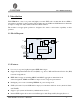
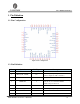
FLC-WFM301 Datasheet 3. Pin Definition 3.1 Pin Configuration Figure 2: Pin Configuration 3.2 Pin Definition Pin Symbol I/O Type 1 GND Ground 2 GPIO[5] (BT_STATE) I/O General Purpose Input/Output (Can be configured for BT coexistence ) 3 NC1 I/O NC 4 SLEEPCLK I Sleep Clock Mode: Clock Input for External Sleep Clock, If only use external 32.768KHz.
FLC-WFM301 Datasheet 9 GND 10 WP 11 DEBUG_SPI_MISO 12 NC3 13 14 15 SD_DATA[3] SD_DATA[1] SD_CMD Ground Ground Reserved for Flaircomm used in production. Connect to I2C EEPROM WP pin. Internally pulled high through a 100 k resistor.
FLC-WFM301 Datasheet Power 3.3V Power Supply for AIO[0] – AIO[3] and PIO[8] – PIO[15] 28 VDD_AIO_PIO 29 GPIO[11] 30 VREG_IN_ANA2 Power 1.45V - 2V Analog Power Supply, for internal LDO 31 GND Ground Ground 32 VREG_IN_ANA1 Power 1.45V - 2V Analog Power Supply, for internal LDO 33 GPIO[10] 34 VREG_IN_DIG Power 1.45V - 2V Digital Power Supply, for internal LDO 35 VDD_RF1 Power 3.3V (2.7 – 4.8V) PA Power Supply (for FEM_VCC1 / FEM_VCC2) 36 VDD_RF2 Power 3.3V (2.7 – 4.
FLC-WFM301 Datasheet 4. Physical Interfaces 4.1 Power Supply 4.1.1 Linear Regulators FLC-WFM301 contains four linear regulators: A low-voltage regulator to supply the 1.2V core digital supply Three low-voltage regulators for the 1.2V core auxiliary, radio and RF synthesizer analogue supplies 4.1.2 LDO for Digital Supply VREG_IN_DIG is the input voltage to the internal LDO for digital supply and VDD_DIG is the output of the LDO. A low ESR 2.2uF capacitor to ground should be connected to this pin. 4.1.
FLC-WFM301 Datasheet 4.3 RF Interface The module integrates a band-pass filter to the antenna port which is a 50 port. The user can connect a 50 antenna directly to the antenna port (pin 48). 4.4 General Purpose Digital IO There are nine general purpose digital IOs defined in the module. All these GPIOs can be configured by software to realize various functions, such as button controls, LED displays or interrupt signals to host controller, etc. Do not connect them if not use.
FLC-WFM301 Datasheet SD_DATA[0] SD_DATA[1] SD_DATA[2] SD_DATA[3] DATA: Data line IPQ#: Interrupt RW: Read wait CD: Card detect DAT[0]: Data line 0 DAT[1]: Data line 1 DAT[2]: Date line 2 DAT[3]: Date line 3 DO: Data output IRQ#: Interrupt Not used CS#: Card select MISO: Data output IRQ#: Interrupt Not used CS#: Card select Table 5: Analog IO Usage All four modes provide identical access to on-chip registers and support clock speeds of up to 50MHz for a maximum burst rate of 200Mbits/s (in SD 4-bit mod
FLC-WFM301 Datasheet 4.6.1.2 Host Sleep and Wake-up The normal method for WFM301CL to wake the host up is via the in-band interrupt on SDIO_DATA[1]. This is the dame mechanism that is used to notify the host of received data or interesting events; no explicit sleep signaling is required. An alternative out-of-band mechanism is provided for hosts that cannot utilize the SDIO interrupt as a wake-up signal, e.g. where a separate power-management IC needs to restore power to the host processor.
FLC-WFM301 Datasheet 5. Electrical Characteristic 5.1 WiFi Performance Specifications 5.1.1 DSSS and CCK modulations (802.11b) TX Performance Specifications Frequency range RMS transmit power(a) RMS EVM Spectral mask 1st Sidelobe Spectral mask 2nd Sidelobe RF carrier suppression Center Frequency Tolerance Occupied Bandwidth Min Typical Max IEEE Specification Unit 2400 16 0 -20 18 3.
FLC-WFM301 Datasheet Frequency range Rx sensitivity,6Mbps(a)(b) Rx sensitivity,9Mbps(a)(b) Rx sensitivity,12Mbps(a)(b) Rx sensitivity,18Mbps(a)(b) Rx sensitivity,24Mbps(a)(b) Rx sensitivity,36Mbps(a)(b) Rx sensitivity,48Mbps(a)(b) Rx sensitivity,54Mbps(a)(b) Rx sensitivity,MCS0(a)(c) Rx sensitivity, MCS1(a)(c) Rx sensitivity, MCS2(a)(c) Rx sensitivity, MCS3(a)(c) Rx sensitivity, MCS4(a)(c) Rx sensitivity, MCS5(a)(c) Rx sensitivity, MCS6(a)(c) Rx sensitivity, MCS7(a)(c) Maximum input level(d) Adjacent chann
FLC-WFM301 Datasheet Operating Condition Operating Temperature Range Min Max for A and I grade -40 ºC +85 ºC for V and C grade -20 ºC +70 ºC 1.7V 1.7V 1.45V 3.6V 3.3V 2.0V Host interface I/O supply voltage (VDD_SDIO) Other I/O supply voltage (VDD_PADS_PIO_0_7, VDD_AIO_PIO_8_15) Linear regulator supply voltage (VREG_IN_DIG, VREG_IN_ANA) Table 11: Recommended Operating Conditions 5.2.3 Current Consumption State Power Consumption 135mA @1.8V 10mA @3.3V 160mA @1.8V 155mA @3.3V 66μ A @1.8V 5A @3.
FLC-WFM301 Datasheet Reset assert on VDD_DIG falling(Sleep mode) 0.770 0.785 0.
FLC-WFM301 Datasheet 6.
FLC-WFM301 Datasheet 7. Mechanical Characteristic 1.15±0.05 8.90±0.1 3.05±0.1 8.90±0.1 2.30±0.1 2.30±0.1 3.05±0.1 0.5±0.05 0.6±0.1 1.15±0.05 0.60±0.05 Figure 4: Mechanical Characteristic 0.35±0.
FLC-WFM301 Datasheet 8. Recommended PCB Layout and Mounting Pattern Placement and PCB layout are critical to optimize the performances of a module without on-board antenna designs. The trace from the antenna port of the module to an external antenna should be 50 and must be as short as possible to avoid any interference into the transceiver of the module. The location of the external antenna and RF-IN port of the module should be kept away from any noise sources and digital traces.
FLC-WFM301 Datasheet Distance between connection and ground area on the top layer should at least be as large as the dielectric thickness. Routing the RF close to digital sections of the system board should be avoided. To reduce signal reflections, sharp angles in the routing of the micro strip line should be avoided. Chamfers or fillets are preferred for rectangular routing; 45-degree routing is preferred over Manhattan style 90-degree routing.
FLC-WFM301 Datasheet 9. Recommended Reflow Profile The soldering profile depends on various parameters necessitating a set up for each application. The data here is given only for guidance on solder reflow. ℃ 250 217 210 A 25 0 B 1 2 C 3 D 4 E 5 6 min Figure 9: Recommended Reflow Profile Pre-heat zone (A) — This zone raises the temperature at a controlled rate, typically 0.5 – 2 C/s. The purpose of this zone is to preheat the PCB board and components to 120 ~ 150 C.
FLC-WFM301 Datasheet 10. Ordering Information 10.1 Product Packaging Information Figure 10: Product Packaging Information 10.2 Ordering information FLC-WFM301XYZA Product Revision Shipping Package Product Package Product Grade Figure 11: Ordering Information 10.2.1 Product Revision Product Revision Description Availability A With CSR6027 Yes B With CSR6030 Yes Table 16: Product Revision 10.2.
FLC-WFM301 Datasheet C Connector No Table 18: Product Package 10.2.
FLC-WFM301 Datasheet 11. Cautions &Warnings 11.1 FCC Statement 1. This device complies with Part 15 of the FCC Rules. Operation is subject to the following two conditions: (1) This device may not cause harmful interference. (2) This device must accept any interference received, including interference that may cause undesired operation. 2. Changes or modifications not expressly approved by the party responsible for compliance could void the user's authority to operate the equipment.
FLC-WFM301 Datasheet The packaging of host system that uses WFM301 should display a label indicating the information as follows: Contains FCC ID: P4IWFM301 Model: FLC-WFM301 (with CSR6030) (Series models: FLC-WFM301IL2B/FLC-WFM301VL2B/FLC-WFM301CL2B) Any similar wording that expresses the same meaning may also be used. 11.4 FLC-BTM301 Antenna Statement 11.4.1 Antenna Electrical Specifications Part Number Frequency Range (GHz) Temperature Average Gain VSWR Impedance ALA931C5 2.4~ 2.485 21.5°C typ.
FLC-WFM301 Datasheet Figure 12: ALA931C5 Radiation Pattern : Azimuth@2.
FLC-WFM301 Datasheet Figure 13: ALA931C5 Radiation Pattern : Elevation1@2.
FLC-WFM301 Datasheet Figure 14: ALA931C5 Radiation Pattern : Elevation2@2.