
User's Manual

268XA
Service Manual
2-34
The channel scanner relays select the desired channel to be measured and route it to the
function relays. The function relays route the signal to the appropriate portion of the
Signal Conditioning circuitry, depending on the function being measured (V ac, V dc,
ohms, etc.). The Signal Conditioning circuitry converts the signal into a form that can be
measured by the A/D (i.e., a dc voltage with a range of -3 to 3 V).
The A/D converts the analog voltage to a digital value, which is then read by the A3U5
A/D microprocessor. The box labeled A/D microprocessor represents the microcontroller
and its associated memory and glue logic, upon which the inguard software runs. It
controls all of the other hardware elements on the inguard and handles communication
with the outguard.
The primary task of the inguard software is to interpret configuration information and
scan requests from the outguard, manipulate the hardware in the appropriate way to
obtain the requested measurements, and return the measurement data to the outguard.
Hardware Elements
This section contains information about the various hardware subsystems on the inguard
board.
Channel MUX
The channel multiplexing consists of treeing and channel switches, implemented with
either FET switches (FAI) or reed relays (PAI). There are two sets of bits associated with
these switches. The tree bits must be set to indicate which bank of channels is being used
where bank 0 is channels 1 to 10, and bank 1 is channels 11-20. For four-wire ohms
measurements, both banks are selected. The position of the tree switches is also a
function of the channel function and range being measured.
The channel bits are set to indicate which of the 10 channels within a bank is being
selected. To deselect a channel (so that no channels are selected), write 1111 to the
channel bits. The tree bits should not be deselected, since this would result in excessive
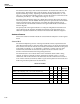
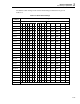
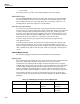
wear of these switches (for the PAI). Table 2-8 gives the bit patterns for the tree bits and
Table 2-9 gives the bit patterns for the channel bits.
Table 2-8. Tree Bits
Signal TR
2
TR
1
TR
0 Switches
2W Ω, V ac, Frequency, V dc, <=3 V, OTC, TC (CH1-10) 1 0 1 K21, K23
2W Ω, V ac, Frequency, V dc, <=3 V, OTC, TC (CH11-20) 1 1 0 K22, K24
V dc >3 V (CH1-10) 0 0 1 K23
V dc >3 V (CH11-20) 0 1 0 K24
4W Ω 111K21, K24