
User's Manual


Corrective Maintenance
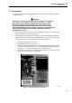
7.3 Charger Circuit 7
7-5
If not correct, then:
a. Check +3V3GAR at the + of C568 or TP571 for +3.3V.
If not correct, possibly caused by V569, R580, + of C568 short to ground, loose
pins of N501, N501 defective.
b. Check N501 pin 8 (VADALOW) for ≅ 1.1V
If not correct:
1. Check R515 and connections.
The P-ASIC supplies a current to R515. The current source uses REFPWM2
and IREF, see 2 and 3 below.
2. Check N501 pin 73 (REFPWM2) for +3V3. REFPWM2 is supplied by the
P-ASIC. Check TP307 (N501 pin 72, REFP) for 1.22V, check V302 and
R307.
3. Check N501 pin 74 (IREF) for 1.61V.
If not correct, possibly caused by R528, loose pin 74, or N501 defective.
c. Check +3V3SADC on N501 pin 65 for +3.3V.
7. Check TP531 (CHARCURR):
The CHARCURR signal controls the battery charge current.
If TP531 < 2.7V continue at step 7a.
If TP531 >2.7V continue at step 7b.
a. Check if charger FET V506 is controlled by a ≅100 kHz, 13 Vpp square wave on
TP502 (FET gate). If correct check/replace V506.
If not correct, check:
1. N501 pin 4 TEMPHI relative to X503 pin 3 (=N501 pin 9) for ≅ 200 mV. If
not correct, check R512 and connections.
2. N501 pin 5 TEMP relative to X503 pin 3 (=N501 pin 9) for ≅ 400...500 mV
at about 20 °C. If not correct check the NTC in the battery pack for ≅12 kΩ
at 20°C (X503 pins 3 and 5); check connections to N501.
3. N501 pin 6 (IMAXCHA) for ≅ 150 mV. If not correct check R514, and
connections to N501.
4. N501 pin 7 (VBATHIGH) for ≅ 1.2V. If not correct check R513, and
connections to N501.
Steps 1 to 4 verify that N501 supplies a 47
μ
A current to each of the resistors
R512, battery NTC, R514, and R513
5. Check N501 pin 9 for the same voltage as on X503 pin 3 (sense resistors
R504, R506, and R507).
6. If 1 to 5 above correct, then N501 is defective.
b. Connect TP531 for a short time (max. 1 minute) to ground, and see if the FET
gate TP502 now shows a 100 kHz pulse signal.
If it does not, continue at step 7d.
If it does, the CHARCURR control signal is not correct, continue at step 7c.
c. Check the CHARCURR control signal:
The CHARCURR voltage on TP531 is controlled by a pulse width modulated
voltage (CHARCUR) from the D-ASIC D471A (pin B8) via R442. The D-ASIC
measures the required signals needed for control, via the Slow ADC.