
User's Manual


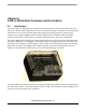

Table Of Contents
- About This Book
- Chapter 1 Safety Information
- Chapter 2 1322x-LPB Module Overview and Description
- Chapter 3 System Overview and Functional Block Descriptions
- Chapter 4 Schematic, Board Layout, and Bill of Materials

1322x-LPB Module Overview and Description
1322x-LPB Reference Manual, Rev. 1.1
2-2 Freescale Semiconductor
2.2 Features
The 1322x-LPB provides the following features:
• Full IEEE 802.15.4 compliant wireless node; ZigBee capable with Freescale’s BeeStack software
stack
• Based on Freescale’s third-generation MC1322x ZigBee platform which incorporates a complete,
low power, 2.4 GHz radio frequency transceiver, 32-bit ARM7 core based MCU, hardware
acceleration for both the IEEE 802.15.4 MAC and AES security, and a full set of MCU peripherals
into a 99-pin LGA Platform-in-Package (PiP)
• MC1322x provides a highly integrated, low cost RF node
— On-board balun and antenna switch in package
— Typical -95 dBm sensitivity
— Typical 0 dBm output power, with max approximately +4 dBm
—F-antenna
• Standard JTAG debug/development interface connector
• Power management circuit with on-board regulation for multiple power sources
— Can be powered from DC power jack, two AAA batteries, or optional Lithium coin cells
— On/Off power switch
— Optional header for measuring MC1322x current
— Power-on green LED
• Supports optional use of buck converter
• User interface switches and LEDs
— 2 push buttons for application purposes
— 2 processor controlled red LEDs for application purposes
— Header for hardware reset
• User interfaces include
— 12-pin GPIO connector provides access to ADC inputs, unbuffered UART2 port, I2C port, and
KBI pins (provide wake-up capabilities from low power)
— 6-pin UART connector provides access to second unbuffer UART1 port
• System clock options
— Default 24 MHz crystal reference oscillator. Supports use of PLL with non-default 13-26 MHz
crystal.
— Optional 32.768 kHz crystal oscillator for accurate real-time delays (crystal is mounted).
• Fixed 1.5 V reference for ADC VREFH during battery operation
• Separate switched VCC (via P-channel MOSFET) for power control of off-chip peripheral
functions.