
Integrated Microcontroller Reference Manual
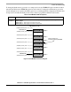

ColdFire Flash Module (CFM)
MCF52211 ColdFire® Integrated Microcontroller Reference Manual, Rev. 2
18-18 Freescale Semiconductor
Therefore, the clock to the flash block timing control, FCLK, is:
FCLK = (input clock) / (DIV + 1)
150KHz < FCLK <= 200KHz
For example, if the input clock frequency is 33 MHz, the CFMCLKD DIV field should be set to 0x14 and
bit PRDIV8 set to 1. The resulting FCLK is 196.4 KHz. As a result, the flash memory program and erase
algorithm timings are increased over the optimum target by:
(200 - 196.4) / 200 x 100% = 1.78%
Remark: INT(X) means taking the integer part of X
Example: INT(33MHz/8/200KHz) = 20
CAUTION
Programming the flash with input clock < 150 KHz should be avoided.
Setting CFMCLKD to a value such that FCLK < 150 KHz can destroy the
flash memory due to overstress. Setting CFMCLKD to a value such that
FCLK > 200 KHz can result in incomplete programming or erasure of the
flash memory array cells.
NOTE
Program and Erase command execution time increases proportionally with
the period of FCLK.
If the CFMCLKD register is written, the DIVLD bit is set automatically. If the DIVLD bit is 0, the
CFMCLKD register has not been written since the last reset. No command can be executed if the
CFMCLKD register has not been written to Section 18.4.2.3.5, “Flash Normal Mode Illegal Operations.”
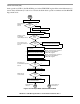
18.4.2.3.2 Command Write Sequence
The flash command controller is used to supervise the command write sequence to execute blank check,
page erase verify, program, page erase, and mass erase algorithms.
Before starting a command write sequence, the ACCERR and PVIOL flags in the CFMUSTAT register
must be clear and the CBEIF flag should be tested to determine the state of the address, data, and command
buffers. If the CBEIF flag is set, indicating the buffers are empty, a new command write sequence can be
executed.
A command write sequence consists of three steps that must be strictly adhered to, because writes to the
CFM are not permitted between steps. However, flash register and array reads are allowed during a
command write sequence. The basic command write sequence is as follows:
1. Write to one or more addresses in the flash memory.
2. Write a valid command to the CFMCMD register.
3. Clear CBEIF flag by writing a 1 to CBEIF to launch the command.
When the CBEIF flag is cleared, the CCIF flag is cleared on the same bus cycle by the flash command
controller indicating that the command was successfully launched. The CBEIF flag is set again indicating
that the address, data, and command buffers are ready for a new command write sequence to begin. A