
Integrated Microcontroller Reference Manual

Analog-to-Digital Converter (ADC)
MCF52211 ColdFire® Integrated Microcontroller Reference Manual, Rev. 2
Freescale Semiconductor 26-25
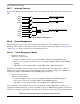
26.5.2 ADC Sample Conversion
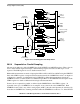
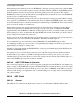
The ADC consists of a cyclic, algorithmic architecture using two recursive sub-ranging sections (RSD#1
and RSD#2), shown in Figure 26-21. Each sub-ranging section resolves a single bit for each conversion
clock, resulting in an overall conversion rate of two bits per clock cycle. Each sub-ranging section is
designed to run at a maximum clock speed of 5.0 MHz. Thus a complete 12-bit conversion takes 6 ADC
clocks (1.2ms), not including sample or post processing time.
Figure 26-21. Cyclic ADC — Top Level Block Diagram
The input mode for a given sample is determined by the CHNCFG field of the CTRL1 register. The ADC
has two input modes:
1. Single-ended mode (CHNCFG bit=0)—In single-ended mode, input mux of the ADC selects one
of the analog inputs and directs it to the plus terminal of the A/D core. The minus terminal of the
A/D core is connected to the V
REFL
reference during this mode. The ADC measures the voltage of
the selected analog input and compares it against the (V
REFH
- V
REFL
) reference voltage range.
2. Differential mode (CHNCFG bit = 1)—In differential mode, the ADC measures the voltage
difference between two analog inputs and compares that against the (V
REFH
- V
REFL
) voltage
range. The input is selected as an input pair: AN0/1, AN2/3, AN4/5, or AN6/7. In this mode, the
plus terminal of the A/D core is connected to the even analog input, while the minus terminal is
connected to the odd analog input.
A mix and match combination of differential and single-ended configurations may exist.
Examples:
• AN0 and AN1 differential, AN2 and AN3 single-ended
• AN4 and AN5 differential, AN6 and AN7 single-ended
Interface
Function
RSD#1
θ
1
RSD#2
θ
2
Cyclic ADC Core
ADCB
MUX
AN3
AN2
AN1
AN0
V+
V
REFL
Channel Select
V–
Single-Ended vs
Differential
Interface
Function
RSD#1
θ
1
RSD#2
θ
2
V+
V–
Cyclic ADC Core
ADCA
AN7
AN6
AN5
AN4
V+
V
REFL
Channel Select
V–
Single-Ended vs
Differential
V+
V–
MUX