
Integrated Microcontroller Reference Manual

Analog-to-Digital Converter (ADC)
MCF52211 ColdFire® Integrated Microcontroller Reference Manual, Rev. 2
Freescale Semiconductor 26-35
26.5.9.2 Description of Clock Operation
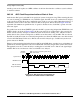
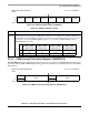
As shown in Figure 26-25, the conversion clock is the primary source for the ADC clock and is always
selected as the ADC clock when conversions are in process. The DIV value in the CTRL2 register should
be configured so the conversion clock frequency falls between 100 kHz and 5.0 MHz. Operating the ADC
at out-of-spec clock frequencies degrades conversion accuracy. Similarly, modifying the parameters affect
clock rates or power modes while the regulators are powered up (PD0=0 or PD1=0) also degrades
conversion accuracy.
The conversion clock ADC uses for sampling is calculated using the IPBus clock and the clock divisor bits
within the CTRL2 register. Please see Section 26.4.1, “Control 1 Register (CTRL1)” or Section 26.4.2,
“Control 2 Register (CTRL2)”. The ADC clock is active 100% of the time while in loop modes, or if power
management is set to normal. It is also active during all ADC power-up for a period of time determined by
the PUDELAY field in the power (POWER) register. After the power-up delay times out, the ADC clock
continues until the completion of the ADCn scan when operating in auto standby or auto power-down
modes.
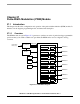
Figure 26-25. ADC Clock Generation
The oscillator clock feeds an 80:1 divider, generating the auto standby clock. The auto standby clock is
selected as the ADC clock during the auto standby power mode when both converters are idle. The auto
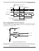
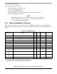
Table 26-22. ADC Clock Summary
Clock input Source Characteristics
Peripheral Clock
(=System Clock)
1/2 Core clock Maximum rate is PLL output divided by 2 if PLL enabled. When PLL disabled,
max rate is oscillator clock divided by 2.
ADC 8MHz Clock Relaxation
Oscillator (8MHz),
Crystal Oscillator
(1-16MHz), or
external Oscillator
Provides 8MHz for auto standby power saving mode.
0
0
1
CTRL2:DIV
(+2 x [DIV+1])
Peripheral (System) Clock
1/2 Core Frequency
0
1
Auto Power-Down
ADC Idle
Disabled (APD=0)
Auto Standby
Enabled (ASB=1)
Standby Current Mode Status
ADC Bit in SIM_PCE
(+80)
Oscillator Clock
(8MHz)
ADC Clock
Auto Standby Clock
(100kHz)
ADC
Conversion
Clock
DIV