
Integrated Microcontroller Reference Manual


Pulse-Width Modulation (PWM) Module
MCF52211 ColdFire® Integrated Microcontroller Reference Manual, Rev. 2
27-14 Freescale Semiconductor
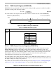
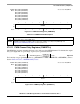
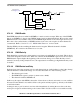
Figure 27-14. PWM Clock Select Block Diagram
27.3.1.1 Prescaled Clock (A or B)
The internal bus clock is the input clock to the PWM prescaler that can be disabled when the device is in
debug mode by setting the PWMCTL[PFRZ] bit. This is useful for reducing power consumption and for
emulation to freeze the PWM. The input clock is also disabled when all PWM channels are disabled
(PWMEn=0).
Clock A and B are scaled values of the input clock. The value is software selectable for clock A and B and
has options of 1, 1/2,..., or 1/128 times the internal bus clock. The value selected for clock A and B is
determined by the PWMPRCLK[PCKAn] and PWMPRCLK[PCKBn] bits.
Internal Bus
Clock (f
sys/
)
PWMSCLA
÷2
1
0
PCLR4
1
0
PCLR5
PWMPRCLK
PWMSCLB
1
0
PCLR2
1
0
PCLR3
[PCKB]
PWMPRCLK
[PCKA]
Clock A
Clock SA
Clock
Clock B
Clock SB
÷2
Clock to
PWM4
Clock to
PWM5
Clock to
PWM2
Clock to
PWM3
1
0
PCLR6
1
0
PCLR7
Clock to
PWM6
Clock to
PWM7
1
0
PCLR0
1
0
PCLR1
Clock to
PWM0
Clock to
PWM1