
User manual


56F8322 Techncial Data, Rev. 10.0
104 Freescale Semiconductor
Preliminary
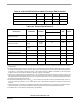
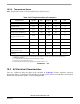
Table 10-6 Power-On Reset Low Voltage Parameters
Characteristic Symbol Min Typ Max Units
POR Trip Point Rising
1
1. Both V
EI2.5
and V
EI3.3
thresholds must be met for POR to be released on power-up.
POR
R
——— V
POR Trip Point Falling
POR
F
1.75 1.8 1.9 V
LVI, 2.5V Supply, trip point
2
2. When V
DD_CORE
drops below V
EI2.5
, an interrupt is generated.
V
EI2.5
—2.14— V
LVI, 3.3V supply, trip point
3
3. When V
DD_CORE
drops below V
EI3.3
, an interrupt is generated.
V
EI3.3
—2.7— V
Bias Current
I
bias
— 110 130 µA
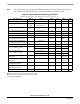
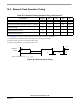
Table 10-7 Current Consumption per Power Supply Pin (Typical)
On-Chip Regulator Enabled (OCR_DIS = Low)
Mode
I
DD_IO
1
1. No Output Switching (Output switching current can be estimated from I = CVf for each output)
2. Includes Processor Core current supplied by internal voltage regulator
I
DD_ADC
I
DD_OSC_PLL
Test Conditions
RUN1_MAC
115mA 25mA 2.5mA
• 60MHz Device Clock
• All peripheral clocks are enabled
• Continuous MAC instructions with fetches from
Data RAM
• ADC powered on and clocked
Wait3
60mA 35µA2.5mA
• 60MHz Device Clock
• All peripheral clocks are enabled
• ADC powered off
Stop1
5.7mA 0µA 360µA
• 4MHz Device Clock
• All peripheral clocks are off
• Relaxation oscillator is on
• ADC powered off
• PLL powered off
Stop2
5mA 0µA 145µA
• Relaxation oscillator is off
• All peripheral clocks are off
• ADC powered off
• PLL powered off