
User manual


Serial Peripheral Interface (SPI) Timing
56F8322 Technical Data, Rev. 10.0
Freescale Semiconductor 115
Preliminary
10.9 Serial Peripheral Interface (SPI) Timing
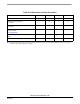
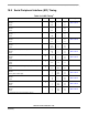
Table 10-18 SPI Timing
1
1. Parameters listed are guaranteed by design.
Characteristic Symbol Min Max Unit See Figure
Cycle time
Master
Slave
t
C
50
50
—
—
ns
ns
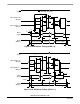
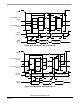
10-9, 10-10,
10-11, 10-12
Enable lead time
Master
Slave
t
ELD
—
25
—
—
ns
ns
10-12
Enable lag time
Master
Slave
t
ELG
—
100
—
—
ns
ns
10-12
Clock (SCK) high time
Master
Slave
t
CH
17.6
25
—
—
ns
ns
10-9, 10-10,
10-11, 10-12
Clock (SCK) low time
Master
Slave
t
CL
16
16.67
—
—
ns
ns
10-12
Data set up time required for inputs
Master
Slave
t
DS
20
0
—
—
ns
ns
10-9, 10-10,
10-11, 10-12
Data hold time required for inputs
Master
Slave
t
DH
0
2
—
—
ns
ns
10-9, 10-10,
10-11, 10-12
Access time (time to data active from high-impedance
state)
Slave
t
A
4.8 15 ns
10-12
Disable time (hold time to high-impedance state)
Slave
t
D
3.7 15.2 ns
10-12
Data Valid for outputs
Master
Slave (after enable edge)
t
DV
—
—
4.5
20.4
ns
ns
10-9, 10-10,
10-11, 10-12
Data invalid
Master
Slave
t
DI
0
0
—
—
ns
ns
10-9, 10-10,
10-11, 10-12
Rise time
Master
Slave
t
R
—
—
11.5
10.0
ns
ns
10-9, 10-10,
10-11, 10-12
Fall time
Master
Slave
t
F
—
—
9.7
9.0
ns
ns
10-9, 10-10,
10-11, 10-12