
User manual

Serial Peripheral Interface (SPI)
MPC8260 PowerQUICC II Family Reference Manual, Rev. 2
38-6 Freescale Semiconductor
mode. Gaps should be inserted between multiple characters to keep from exceeding the maximum
sustained data rate.
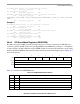
38.4 Programming the SPI Registers
The following sections describe the registers used in configuring and operating the SPI.
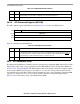
38.4.1 SPI Mode Register (SPMODE)
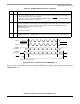
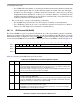
The SPI mode register (SPMODE), shown in Figure 38-4, controls both the SPI operation mode and clock
source.
Table 38-1 describes the SPMODE fields.
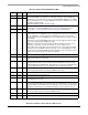
0 1 2 3 4 5 6 7 8 9 101112131415
Field — LOOP CI CP DIV16 REV M/S EN LEN PM
Reset 0000_00
— 0_0000_0000
R/W R/W
Addr 0x0x11AA0
Figure 38-4. SPMODE—SPI Mode Register
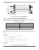
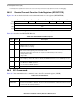
Table 38-1. SPMODE Field Descriptions
Bits Name Description
0 — Reserved, should be cleared.
1 LOOP Loop mode. Enables local loopback operation.
0 Normal operation.
1 Loopback mode. The transmitter output is internally connected to the receiver input. The receiver
and transmitter operate normally, except that received data is ignored.
2 CI Clock invert. Inverts SPI clock polarity. See Figure 38-5 and Figure 38-6.
0 The inactive state of SPICLK is low.
1 The inactive state of SPICLK is high.
3 CP Clock phase. Selects the transfer format. See Figure 38-5 and Figure 38-6.
0 SPICLK starts toggling at the middle of the data transfer.
1 SPICLK starts toggling at the beginning of the data transfer.
4 DIV16 Divide by 16. Selects the clock source for the SPI baud rate generator when configured as an SPI
master. In slave mode, SPICLK is the clock source.
0 BRGCLK is the input to the SPI BRG.
1 BRGCLK/16 is the input to the SPI BRG.
5 REV Reverse data. Determines the receive and transmit character bit order.
0 Reverse data—lsb of the character sent and received first.
1 Normal operation—msb of the character sent and received first.
6 M/S Master/slave. Selects master or slave mode.
0 The SPI is a slave.
1 The SPI is a master.