
User manual

I
2
C Controller
MPC8260 PowerQUICC II Family Reference Manual, Rev. 2
Freescale Semiconductor 39-3
because the R/W request follows the slave port address in the I
2
C bus specification, the R/W request bit
must be placed in the lsb (bit 7) unless operating in reverse data mode; see Section 39.4.1, “I
2
C Mode
Register (I2MOD).”
To write to a slave, the master sends a write request (R/W = 0) along with either the target slave’s address
or a general call (broadcast) address of all zeros, followed by the data to be written. To read from a slave,
the master sends a read request (R/W = 1) and the target slave’s address. When the target slave
acknowledges the read request, the transfer direction is reversed, and the master receives the slave’s
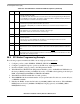
transmit buffer(s). If the receiver (master or slave) does not acknowledge each byte transfer in the ninth
bit frame, the transmitter signals a transmission error event (I2ER[TXE]). An I
2
C transfer timing diagram
is shown in Figure 39-3.
Figure 39-3. I
2
C Transfer Timing
Select master or slave mode for the controller using the I
2
C command register (I2COM[M/S]). Set the
master’s start bit, I2COM[STR], to begin a transfer; setting a slave’s I2COM[STR] activates the slave to
wait for a transfer request from a master.
If a master or slave transmitter’s current TxBD[L] is set, transmission stops once the buffer is sent; that is,
I2COM[STR] must be set again to reactivate transfers. If TxBD[L] is zero, once the current buffer is sent,
the controller begins processing the next TxBD without waiting for I2COM[STR] to be set again.
The following sections further detail the transfer process.
39.3.1 I
2
C Master Write (Slave Read)
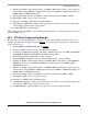
If the PowerQUICC II is the master, prepare the transmit buffers and BDs before initiating a write.
Initialize the first transmit data byte with the slave address and write request (R/W = 0).
If the PowerQUICC II is the slave target of the write, prepare receive buffers and BDs to await the master’s
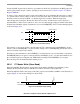
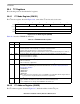
request. Figure 39-4 shows the timing for a master write.
Figure 39-4. I
2
C Master Write Timing
SCL
SDA
Data Byte
Start Condition Stop Condition
A
C
K
789456123
SDA Device Address
W
Data Byte
S
T
A
R
T
S
T
O
P
A
C
K
A
C
K
Note: Data and ACK are repeated n times.