
User manual

I
2
C Controller
MPC8260 PowerQUICC II Family Reference Manual, Rev. 2
39-6 Freescale Semiconductor
39.4 I
2
C Registers
The following sections describe the I
2
C registers.
39.4.1 I
2
C Mode Register (I2MOD)
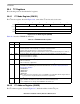
The I
2
C mode register, shown in Figure 39-6, controls the I
2
C modes and clock source.
Table 39-1 describes I2MOD bit functions.
39.4.2 I
2
C Address Register (I2ADD)
The I
2
C address register, shown in Figure 39-7, holds the address for this I
2
C port.
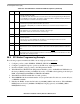
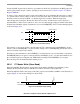
01234567
Field — REVD GCD FLT PDIV EN
Reset 0000_0000
R/W R/W
Addr 0x0x11860
Figure 39-6. I
2
C Mode Register (I2MOD)
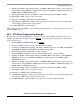
Table 39-1. I
I2MOD Field Descriptions
Bits Name Description
0–1 — Reserved and should be cleared.
2 REVD Reverse data. Determines the Rx and Tx character bit order.
0 Normal operation. The msb (bit 0) of a character is transferred first.
1 Reverse data. the lsb (bit 7) of a character is transferred first.
Note: Clearing REVD is strongly recommended to ensure consistent bit ordering across devices.
3 GCD General call disable. Determines whether the receiver acknowledges a general call address.
0 General call address is enabled.
1 General call address is disabled.
4 FLT Clock filter. Determines if the I
2
C input clock SCL is filtered to prevent spikes in a noisy environment.
0 SCL is not filtered.
1 SCL is filtered by a digital filter.
5–6 PDIV Predivider. Selects the clock division factor before it is input into the I
2
C BRG. The clock source for
the I
2
C BRG is the BRGCLK generated from the CPM clock; see Section 10.8, “System Clock
Control Register (SCCR).”
00 BRGCLK/32
01 BRGCLK/16
10 BRGCLK/8
11 BRGCLK/4
Note: To both save power and reduce noise susceptibility, select the PDIV with the largest division
factor (slowest clock) that still meets performance requirements.
7 EN Enable I
2
C operation.
0I
2
C is disabled. The I
2
C is in a reset state and consumes minimal power.
1I
2
C is enabled. Do not change other I2MOD bits when EN is set.