
User manual

Parallel I/O Ports
MPC8260 PowerQUICC II Family Reference Manual, Rev. 2
Freescale Semiconductor 40-5
PSOR bits are effective only if the corresponding PPARx[DDx] = 1 (a dedicated peripheral function).
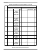
Table 40-4 describes PSORx fields.
NOTE
If the corresponding PPARx[DDx] = 1 (configured as a general-purpose pin)
before programming a PSORx or PDIRx bit, a pin might function for a short
period as an unwanted dedicated function and cause unknown behavior.
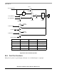
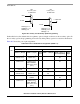
40.3 Port Block Diagram
Figure 40-6 shows the functional block diagram.
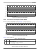
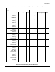
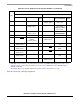
0123456789101112131415
Field SO0
1
SO1
1
SO2
1
SO3
1
SO4 SO5 SO6 SO7 SO8 SO9 SO10 SO11 SO12 SO13 SO14 SO15
Reset 0000_0000_0000_0000
R/W R/W
Addr 0x0x10D08 (PSORA), 0x0x10D28 (PSORB), 0x0x10D48 (PSORC), 0x0x10D68 (PSORD)
16 17 18 19 20 21 22 23 24 25 26 27 28 29 30 31
Field SO16 SO17 SO18 SO19 SO20 SO21 SO22 SO23 SO24 SO25 SO26 SO27 SO28 SO29 SO30 SO31
Reset 0000_0000_0000_0000
R/W R/W
Addr 0x10D0A (PSORA), 0x10D2A (PSORB), 0x10D4A (PSORC), 0x10D6A (PSORD)
1
These bits are valid for PSORA and PSORC only
Figure 40-5. Special Options Registers (PSORA–POSRD)
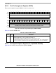
Table 40-4. PSOR
x
Field Descriptions
Bits Name Description
0–31 SO
x
Special-option. Determines whether a pin configured for a dedicated function (PPAR
x
[DD
x
] = 1)
uses option 1 or option 2. Note that bits SO0–SO3 are valid for PSORA and PSORC only. Options
are described in Section 40.2, “Port Registers.”
0 Dedicated peripheral function. Option 1.
1 Dedicated peripheral function. Option 2.