
User manual

Parallel I/O Ports
MPC8260 PowerQUICC II Family Reference Manual, Rev. 2
40-14 Freescale Semiconductor
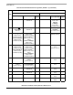
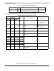
Table 40-7 shows the port C pin assignments.
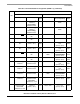
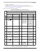
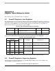
PB6 FCC3: TXD[1]
MII/HDLC nibble
FCC2: RxD[2]
1
UTOPIA 8
(primary option)
by
PC11
TDM_A2: L1RXD
Inout, serial
TDM_A2: L1RXD[0]
Input, nibble
(primary option)
by
PD21
PB5 FCC3: TXD[2]
MII/HDLC nibble
FCC2: RxD[1]
1
UTOPIA 8
(primary option)
by
PD10
TDM_A2:
L1TSYNC/GRANT
(primary option)
by PC9
PB4 FCC3: TXD[3]
MII/HDLC nibble
FCC2: RxD[0]
1
UTOPIA 8
(primary option)
by
PD11
FCC3: RTSN TDM_A2: L1RSYNC
(primary option)
by
PD20
1
Not available on the MPC8250.
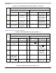
Table 40-7. Port C Dedicated Pin Assignment (PPARC = 1)
PIN
Pin Function
PSORC = 0 PSORC = 1
PDIRC = 1 (Output) PDIRC = 0 (Input)
Defaul
t Input
PDIRC = 1 (Output)
PDIRC = 0 (Input or
Inout if Specified)
Defaul
t Input
PC31 BRG1: BRGO CLK1 CLK5
PC30 FCC2: TxD[3]
1
UTOPIA 8
CLK2 CLK6 Timer1:TOUT
PC29 BRG2: BRGO CLK3/TIN2 CLK7 SCC1: CTS
2
SCC1: CLSN
2
Ethernet
(secondary option)
GND
PC28 Timer2: TOUT CLK4/TIN1 CLK8 SCC2: CTS
2
SCC2: CLSN
2
Ethernet
(secondary option)
GND
PC27 FCC3: TxD
HDLC/transp. serial
FCC3: TxD[0]
MII/HDLC nibble
CLK5 GND BRG3: BRGO
PC26 Timer3: TOUT CLK6 GND TMCLK
real-time counter
BRGO
1
Table 40-6. Port B Dedicated Pin Assignment (PPARB = 1) (continued)
Pin
Pin Function
PSORB = 0 PSORB = 1
PDIRB = 1 (Output) PDIRB = 0 (Input)
Defaul
t Input
PDIRB = 1 (Output)
PDIRB = 0 (Input or
Inout if Specified)
Defaul
t Input