
User manual

System Interface Unit (SIU)
MPC8260 PowerQUICC II Family Reference Manual, Rev. 2
4-34 Freescale Semiconductor
2 PBSE Parity byte select enable.
0 Parity byte select is disabled. GPL4 output of UPM is available for memory control.
1 Parity byte select is enabled. GPL4 pin is used as parity byte select output from the
PowerQUICC II.
Note: Should not be set if BRx[DECC] = 00. Refer to Section 11.3.1, “Base Registers (BRx).”
3 CDIS Core disable.
0 The PowerQUICC II core is enabled.
1 The PowerQUICC II core is disabled. PowerQUICC II functions as a slave device.
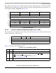
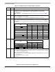
4–5 DPPC Data parity pins configuration. Note that the additional arbitration lines (EXT_BR2, EXT_BG2,
EXT_DBG2, EXT_BR3, EXT_BG3, and EXT_DBG3) are operational only when ACR[EARB] = 0.
Setting EARB (to choose external arbiter) combined with programming DPPC to 11 deactivates
these lines.
Pin
DPPC
00 01 10 11
DP(0)/RSRV
— DP(0) RSRV EXT_BR2
DP(1)/IRQ1
IRQ1 DP(1) IRQ1 EXT_BG2
DP(2)/TLBISYNC
/IRQ2 IRQ2 DP(2) TLBISYNC EXT_DBG2
DP(3)/IRQ3
IRQ3 DP(3) CKSTP_OU
T
EXT_BR3
DP(4)/IRQ4
IRQ4 DP(4) CORE_SRE
SET
EXT_BG3
DP(5)/TBEN/IRQ5
IRQ5 DP(5) TBEN EXT_DBG3
DP(6)/CSE(0)/IRQ6
IRQ6 DP(6) CSE(0) IRQ6
DP(7)/CSE(1)/IRQ7
IRQ7 DP(7) CSE(1) IRQ7
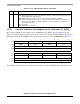
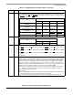
6–7 L2CPC L2 cache pins configuration.
Pin
Multiplexing
L2CPC = 00 L2CPC = 01 L2CPC = 10
CI
/BADDR(29)/IRQ2 CI IRQ2 BADDR(29)
WT
/BADDR(30)/IRQ3 WT IRQ3 BADDR(30)
L2_HIT
/IRQ4 L2_HIT IRQ4 —
CPU_BG
/BADDR(31)/IRQ5 CPU_BG IRQ5 BADDR(31)
8–9 LBPC Local bus pins configuration.
Note: LBPC should be programmed only during the hard reset configuration sequence (using the
hard reset configuration word).
00 Local bus pins function as local bus
01 Local bus pins function as PCI bus (MPC8250, MPC8265, and MPC8266 only). Reserved on
all other devices.
10 Local bus pins function as core pins
11 Reserved
Table 4-12. SIUMCR Register Field Descriptions (continued)
Bits Name Description