
User manual
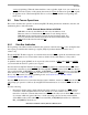

The 60x Bus
MPC8260 PowerQUICC II Family Reference Manual, Rev. 2
8-18 Freescale Semiconductor
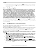
8.4.3.7 60x-Compatible Bus Mode—Size Calculation
To comply with the requirements listed in Table 8-6 and Table 8-7, the transfer size and a new address must
be calculated at the termination of each beat of a port-size transaction. In single-PowerQUICC II bus
mode, these calculations are internal and do not constrain the system. In 60x-compatible bus mode, the
external slave or master must determine the new address and size. Table 8-9 describes the address and size
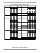
Table 8-8. Data Bus: Read Cycle Requirements and Write Cycle Content
Transfer
Size
TSIZ[0–3]
Address
State
1
A[29–31]
1
Address state is the calculated address for port size.
Port Size/Data Bus Assignments
64-Bit 32-Bit 16-Bit 8-Bit
0–7 8–15 16–23 24–31 32–39 40–47 48–55 56–63 0–7 8–15 16–23 24–31 0–7 8–15 0–7
Byte
(0001)
000 OP0
2
2
OP
n
: These lanes are read or written during that bus transaction. OP0 is the most-significant byte of a word operand
and OP7 is the least-significant byte.
—
3
3
— These lanes are ignored during read cycles and driven with undefined data during write cycles.
——————OP0— — —OP0—OP0
001 —OP1———————OP1— — —OP1OP1
010 — — OP2 — — — — — — — OP2 — OP2 — OP2
011 — ——OP3—————— —OP3—OP3OP3
100 — — — — OP4 — — — OP4 — — — OP4 — OP4
101 — — — — — OP5 — — — OP5 — — — OP5 OP5
110 — — — — — — OP6 — — — OP6 — OP6 — OP6
111 — ——————OP7—— —OP7—OP7OP7
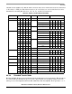
Half Word
(0010)
000 OP0 OP1 — — — — — — OP0 OP1 — — OP0 OP1 OP0
001 — OP1 OP2 — — — — — — OP1 OP2 — — OP1 OP1
010 — — OP2 OP3 — — — — — — OP2 OP3 OP2 OP3 OP2
100 — — — — OP4 OP5 — — OP4 OP5 — — OP4 OP5 OP4
101 — — — — — OP5 OP6 — — OP5 OP6 — — OP5 OP5
110 — — — — — — OP6 OP7 — — OP6 OP7 OP6 OP7 OP6
Tr i p l e B y t e
(0011)
000 OP0 OP1 OP2 — — — — — OP0 OP1 OP2 — OP0 OP1 OP0
001 — OP1 OP2 OP3 — — — — — OP1 OP2 OP3 — OP1 OP1
100 — — — — OP4 OP5 OP6 — OP4 OP5 OP6 — OP4 OP5 OP4
101 — — — — — OP5 OP6 OP7 — OP5 OP6 OP7 — OP5 OP5
Word
(0100)
000 OP0 OP1 OP2 OP3 — — — — OP0 OP1 OP2 OP3 OP0 OP1 OP0
100 — — — — OP4 OP5 OP6 OP7 OP4 OP5 OP6 OP7 OP4 OP5 OP4
Double
Word
(0000)
000 OP0 OP1 OP2 OP3 OP4 OP5 OP6 OP7 OP0 OP1 OP2 OP3 OP0 OP1 OP0