
User manual

The 60x Bus
MPC8260 PowerQUICC II Family Reference Manual, Rev. 2
8-20 Freescale Semiconductor
16-, or 24-byte extended transfers. These transactions are compatible with the 60x bus, but some slaves or
masters do not support these features. Clear BCR[ETM] to disable this type of transaction. This places the
PowerQUICC II in strict 60x bus mode. The following tables are extensions to Table 8-7, Table 8-8, and
Table 8-9.
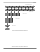
Table 8-10 lists the patterns of the extended data transfer for write cycles when PowerQUICC II initiates
an access. Note that 16- and 24-byte transfers are always eight-byte aligned and use a 64-bit or less port
size.
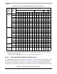
Table 8-11 lists the bytes required on the data bus for extended read cycles. Note that 16- and 24-byte
transfers are always 8-byte aligned and use a maximum 64-bit port size.
Table 8-12 includes added states to the transfer size calculation state machine. Only extended transfers use
these states.
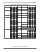
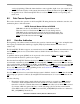
Table 8-10. Data Bus Contents for Extended Write Cycles
Transfer
Size
TSIZ[0–3])
Address
State
A[29–31]
External Data Bus Pattern
D[0–7] D[8–15] D[16–23] D[24–31] D[32–39] D[40–47] D[48–55] D[56–63]
5 Bytes
(0101)
000 OP0 OP1 OP2 OP3 OP4 — — —
011 OP3 OP3 — OP3 OP4 OP5 OP6 OP7
6 Bytes
(0110)
000 OP0 OP1 OP2 OP3 OP4 OP5 — —
010 OP2 OP3 OP2 OP3 OP4 OP5 OP6 OP7
7 Bytes
(0111)
000 OP0 OP1 OP2 OP3 OP4 OP5 OP6 —
001 OP1 OP1 OP2 OP3 OP4 OP5 OP6 OP7
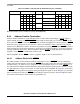
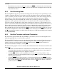
Table 8-11. Data Bus Requirements for Extended Read Cycles
Transfer
Size
TSIZ[0–3]
Addres
s State
A[29-31
]
Port Size/Data Bus Assignments
64-Bit 32-Bit 16-Bit 8-Bit
0–7 8–15 16–2
3
24–3
1
32–3
9
40–4
7
48–5
5
56–6
3
0–7 8–15 16–2
3
24–3
1
0–7 8–15 0–7
5 Byte
(0101)
000 OP
0
OP
1
OP2 OP3 OP4 — — — OP
0
OP1 OP2 OP3 OP0 OP1 OP0
011 — — — OP3 OP4 OP5 OP6 OP7 — — — OP3 — OP3 OP3
6 Byte
(0110)
000 OP
0
OP
1
OP2 OP3 OP4 OP5 — — OP
0
OP1 OP2 OP3 OP0 OP1 OP0
010 — — OP2 OP3 OP4 OP5 OP6 OP7 — — OP2 OP3 OP2 OP3 OP2
7 Byte
(0111)
000 OP
0
OP
1
OP2 OP3 OP4 OP5 OP6 — OP
0
OP1 OP2 OP3 OP0 OP1 OP0
001 — OP
1
OP2 OP3 OP4 OP5 OP6 OP7 — OP1 OP2 OP3 — OP1 OP1