
User manual

PCI Bridge
MPC8260 PowerQUICC II Family Reference Manual, Rev. 2
9-52 Freescale Semiconductor
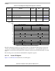
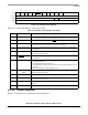
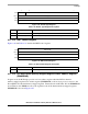
Figure 9-41. PCI Bus Cache Line Size Register
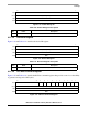
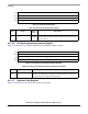
9.11.2.10 PCI Bus Latency Timer Register
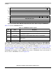
Figure 9-42 and Table 9-29 describe the PCI bus latency timer register.
Figure 9-42. PCI Bus Latency Timer Register
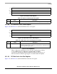
9.11.2.11 Header Type Register
Figure 9-43 and Table 9-30 describe the header type register.
7 0
Field CLS
Reset 0000_0000
R/W R/W
Addr 0x0C
Table 9-28. PCI Bus Cache Line Size Register Description
Bits Name Description
7–0 Cache line size Represents the cache line size of the system in terms of 32-bit words (eight 32-bit
words = 32 bytes). This register is read-write; however, an attempt to program this
register to any value other than 8 results in it being cleared.
7320
Field LT LT
Reset 0000_0000
R/W R/W R
Addr 0x0D
Table 9-29. PCI Bus Latency Timer Register Description
Bits Name Description
7–3 Latency timer Represents the maximum number of PCI clocks that the device, when mastering
a transaction, holds the bus after PCI bus grant has been negated. The value is
in PCI clocks. Refer to the PCI 2.2 specification for the rules by which the PCI bus
interface unit completes transactions when the timer has expired.
2–0 Read-only least-significant bits of the latency timer. (The latency timer value is
programmed in multiples of eight.)