
User manual

PCI Bridge
MPC8260 PowerQUICC II Family Reference Manual, Rev. 2
9-58 Freescale Semiconductor
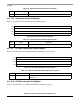
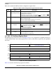
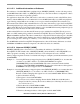
9.11.2.21 PCI Bus MAX LAT
Figure 9-53 and Table 9-40 describe the PCI bus MAX LAT register.
Figure 9-53. PCI Bus MAX LAT
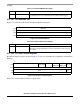
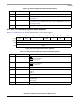
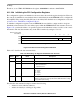
9.11.2.22 PCI Bus Function Register
The PCI bus function register, shown in Figure 9-54, is used to determine the configuration of the PCI bus
interface.
Figure 9-54. PCI Bus Function Register
Table 9-41. describes PCI bus function register fields.
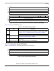
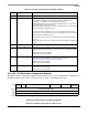
Table 9-39. PCI Bus MIN GNT Description
Bits Name Description
7–0 MIN GNT Specifies the length of the device’s burst period. The value 0x00 indicates that
the PCI bridge has no major requirements for the settings of latency timers.
7 0
Field MAX LAT
Reset 0000_0000
R/W R
Addr 0x3F
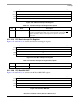
Table 9-40. PCI Bus MAX LAT Description
Bits Name Description
7–0 MAX LAT Specifies how often the device needs to gain access to the PCI bus. The value
0x00 indicates that the PCI bridge has no major requirements for the settings of
latency timers.
15 6 5 4 3 2 1 0
Field — CFG_LOCK —
TRGT_
LATENCY_DIS
MSTR_
LATENCY_DIS
PCI_HA
Reset 0000_0000_0010_0000
R/W R/W R
Addr 0x44