
User manual

Clocks and Power Control
MPC8260 PowerQUICC II Family Reference Manual, Rev. 2
Freescale Semiconductor 10-7
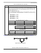
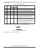
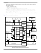
Figure 10-4 shows the filtering circuit for VCCSYN and VCCSYN1, described in Table 10-1.
Figure 10-4. PLL Filtering Circuit
XFC External filter capacitor—Connects to the off-chip capacitor for the main PLL filter. One terminal of the
capacitor is connected to XFC while the other terminal is connected to VCCSYN. 30 MΩ is the minimum
parasitic resistance value that ensures proper PLL operation when connected in parallel with the XFC
capacitor. A multiplication factor (MF) based on CPM_CLK/CLKIN determines the XFC capacitor value
according to the following tables:
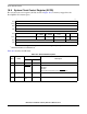
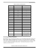
Definition of Multiplication Factor (MF)
If the ratio of CPM_CLK/CLKIN is an integer (A), MF = A. If CPM_CLK/CLKIN is A.5, MF = 2 x A.5. For
example, if CPM_CLK/CLKIN is 166.66 MHz/ 66.66 MHz = 2.5, then MF = 5. The relevant factors are as
follows:
CPM_CLK/CLKIN = 2 MF = 2
CPM_CLK/CLKIN = 2.5 MF = 5
CPM_CLK/CLKIN = 3 MF = 3
CPM_CLK/CLKIN = 3.5 MF = 7
CPM_CLK/CLKIN = 4 MF = 4
CPM_CLK/CLKIN = 5 MF = 5
CPM_CLK/CLKIN = 6 MF = 6
Table 10-1. Dedicated PLL Pins (continued)
Signal Description
.29µm (HiP3) Silicon: Rev. A.1 and B.x
Multiplication Factor Maximum Allowed Capacitance Minimum Allowed Capacitance Unit
MF ≤ 4 MF x 840 - 90 MF x 750 - 90 pF
MF > 4 MF x 1220 MF x 1100 pF
.29µm (HiP3) Silicon: Rev. C.2 and Future Revisions
Maximum Allowed Capacitance Minimum Allowed Capacitance Unit
MF x 840 - 90 MF x 750 - 90 pF
.25µm (HiP4) Silicon
Recommended
Capacitance
Maximum Allowed Capacitance Minimum Allowed Capacitance Unit
MF x 680 - 120 MF x 780 - 140 MF x 580 -100 pF
10 Ω
VDD
0.1 µF
10 µF
VCCSYN