
User manual

Clocks and Power Control
MPC8260 PowerQUICC II Family Reference Manual, Rev. 2
10-8 Freescale Semiconductor
10.8 System Clock Control Register (SCCR)
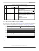
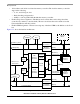
The system clock control register (SCCR), shown in Figure 10-5, is memory-mapped into the
PowerQUICC II’s internal space.
Table 10-2 describes SCCR fields.
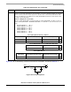
0 15
Field —
Reset —
R/W R/W
Addr 0x0x10C80
16 22 23 24 25 28 29 30 31
Field —
PCI_MODE
1
1
MPC8250, MPC8265, and MPC8266 only.
PCI_MODCK
1
PCIDF
1
CLPD DFBRG
Reset —
0
——
001
R/W R/W R R/W
Addr 0x10C82
Figure 10-5. System Clock Control Register (SCCR)
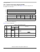
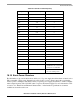
Table 10-2. SCCR Field Descriptions
Bits Name
Defaults
Description
POR Hard Reset
0–22 — 0 Unaffected Reserved
23 PCI_MODE
1
PCI_Mode Unaffected PCI Mode
0 Disabled
1 Enabled
Reflects the inverted value of the PCI_Mode
pin.
24 PCI_MODCK
1
PCI_MODC
K
Unaffected Reflects the value of the PCI_MODCK pin.
25–28 PCIDF
1
Configuratio
n pins
Unaffected PCI division factor.