
User manual

Clocks and Power Control
MPC8260 PowerQUICC II Family Reference Manual, Rev. 2
Freescale Semiconductor 10-11
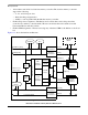
10.10 Basic Power Structure
The I/O buffers, logic, and clock block are fed by a 3.3-V power supply that allows them to function in a
TTL-compatible voltage range. Internal logic can be fed by a lower voltage source; this considerably
reduces power consumption. The PLL is fed by a separate power supply (VCCSYN) to achieve a highly
stable output frequency. The VCCSYN value is equal to the internal supply. For more information, refer
to Section 1.2, “Electrical and Thermal Characteristics,” in the hardware specifications document
available at wwww.freescale.com.
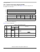
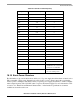
Table 10-4. 60x Bus-to-Core Frequency
SCMR[CORECNF] Bus-to-Core Multiplier VCO Divider
0x02 1x 8
0x01 1x 4
0x0C 1.5x 8
0x00 1.5x 4
0x05, 0x15 2x 4
0x04 2x 2
0x11 2.5x 4
0x06 2.5x 2
0x10 3x 4
0x08 3x 2
0x0E,0x1E 3.5x 2
0x0A, 0x1A 4x 2
0x07, 0x17 4.5x 2
0x0B, 0x1B 5x 2
0x09, 0x19 5.5x 2
0x0D, 0x1D 6x 2
0x12, 6.5x 2
0x14 7x 2
0x16 7.5x 2
0x1C 8x 2
0x03, 0x13 PLL off/bypassed • PLL off
• SYSCLK clocks core directly
• 1x bus-to-core defaulted
0x0F, 0x1F PLL off • PLL off
• no core clocking occurs