
User manual

Memory Controller
MPC8260 PowerQUICC II Family Reference Manual, Rev. 2
Freescale Semiconductor 11-5
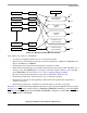
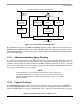
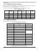
Figure 11-2. Memory Controller Machine Selection
Some features are common to all machines.
• A 17-bit most-significant address decode on each memory bank
• The block size of each memory bank can vary between 32 Kbytes (1 Mbyte for SDRAM) and 4
Gbytes (128 Mbytes for SDRAM).
• Normal parity may be generated and checked for any memory bank.
• Read-modify-write parity may be generated and checked for any memory bank with either 32- or
64-bit port size. Using RMW parity on 32-bit port size bank, requires the bus to be in strict 60x
mode (BCR[ETM] = 0. See Section 4.3.2.1, “Bus Configuration Register (BCR).”
• ECC may be generated and checked for any memory bank with a 64-bit port size
• Each memory bank can be selected for read-only or read/write operation.
• Each memory bank can use data pipelining, which reduces the required data setup time for
synchronous devices.
• Each memory bank can be controlled by an external memory controller or bus slave.
The memory controller functionality minimizes the need for glue logic in PowerQUICC II-based systems.
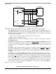
In Figure 11-3, CS0 is used with the 16-bit boot EPROM with BR0[MS] defaulting to select the GPCM.
CS1 is used as the RAS signal for 64-bit DRAM with BR1[MS] configured to select UPMA. BS[0–7] are
used as CAS signals on the DRAM.
User-Programmable
Local General-Purpose
Bank 0
Bank 1
Bank 2
Bank 3
Bank 10
Bank11
MS
MS
MS
MS
MS
MS
Chip-Select Machine
Local SDRAM
Local
60x
Local
M
x
MR[BS]
60x SDRAM
60x
Local
60x General-Purpose
Chip-Select Machine
60x
Machine (A/B/C)
Machine
Machine