
User manual


Memory Controller
MPC8260 PowerQUICC II Family Reference Manual, Rev. 2
Freescale Semiconductor 11-17
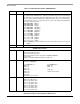
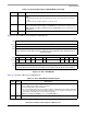
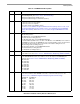
Figure 11-8 shows ORx as it is formatted for GPCM mode.
Table 11-6 describes ORx fields in GPCM mode.
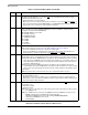
26 PMSEL Page mode select. Selects page mode for the SDRAM connected to the memory controller
bank.
0 Back-to-back page mode (normal operation). Page is closed when the bus becomes
idle.
1 Page is kept open until a page miss or refresh occurs.
27 IBID Internal bank interleaving within same device disable. Setting this bit disables bank
interleaving between internal banks of a SDRAM device connected to the chip-select line.
IBID should be set in 60x-compatible mode if the SDRAM device is not connected to the
BANKSEL pins.
28–31 — Reserved, should be cleared.
0 15
Field AM
Reset
1
1111_1110_0000_0000
1
R/W R/W
Addr 0x0x10104 (OR0); 0x0x1010C (OR1); 0x0x10114 (OR2); 0x0x1011C (OR3); 0x0x10124 (OR4); 0x0x1012C
(OR5); 0x0x10134 (OR6); 0x0x1013C (OR7); 0x0x10144 (OR8); 0x0x1014C (OR9); 0x0x10154 (OR10);
0x0x1015C (OR11)
16 17 18 19 20 21 22 23 24 27 28 29 30 31
Field AM — BCTLD CSNT ACS — SCY SETA TRLX EHTR —
Reset
1
00001110 1111 0100
R/W R/W
Addr 0x10106 (OR0); 0x1010E (OR1); 0x10116 (OR2); 0x1011E (OR3); 0x10126 (OR4); 0x1012E (OR5);
0x10136 (OR6); 0x1013E (OR7); 0x10146 (OR8); 0x1014E (OR9); 0x10156 (OR10); 0x1015E (OR11)
1
Reset values are for OR0 only. OR1–11 are undefined at reset.
Figure 11-8. OR
x
—GPCM Mode
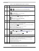
Table 11-6. OR
x
—GPCM Mode Field Descriptions
Bits Name Description
0–16 AM Address mask. Masks corresponding BR
x
bits. Masking address bits independently allows external
devices of different size address ranges to be used.
0 Corresponding address bits are masked.
1 The corresponding address bits are used in the comparison with address pins. Address mask bits
can be set or cleared in any order in the field, allowing a resource to reside in more than one area
of the address map. AM can be read or written at any time.
Note: After system reset, OR0[AM] is 1111_1110_0000_0000_0.
17–18 — Reserved, should be cleared.
Table 11-5. OR
x
Field Descriptions (SDRAM Mode) (continued)
Bits Name Description