
User manual

Memory Controller
MPC8260 PowerQUICC II Family Reference Manual, Rev. 2
Freescale Semiconductor 11-33
11.3.13 60x Bus Error Status and Control Registers (TESCR
x
)
These registers indicate the source of an error that caused TEA or MCP to be asserted on the 60x bus. See
Section 4.3.2.10, “60x Bus Transfer Error Status and Control Register 1 (TESCR1),” and Section 4.3.2.11,
“60x Bus Transfer Error Status and Control Register 2 (TESCR2).”
11.3.14 Local Bus Error Status and Control Registers (L_TESCR
x
)
These registers indicate the source of an error that causes TEA or MCP to be asserted on the local bus. See
Section 4.3.2.12, “Local Bus Transfer Error Status and Control Register 1 (L_TESCR1),” and
Section 4.3.2.13, “Local Bus Transfer Error Status and Control Register 2 (L_TESCR2).”
11.4 SDRAM Machine
The PowerQUICC II provides one SDRAM interface (machine) for the 60x bus and one for the local bus.
The machines provide the necessary control functions and signals for JEDEC-compliant SDRAM devices.
Each bank can control a SDRAM device on the 60x or the local bus. Table 11-18 describes the SDRAM
interface signals controlled by the memory controller.
Additional controls are available in 60x-compatible mode (60x bus only):
• ALE—External address latch enable
• PSDAMUX—External address multiplexing control (asserted = row, negated = column)
Throughout this section, whenever a signal is named, the reference is to the 60x or local bus signal,
according to the accessed bank’s machine-select.
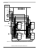
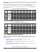
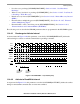
Figure 11-19. shows an eight-bank, 128-Mbyte system. Each bank consists of eight 2 x 1-Mbit x 8
SDRAMs. Note that the SDRAM memory clock must operate at the same frequency as, and be
phase-aligned with, the system clock.
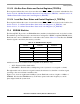
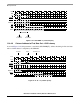
Table 11-18. SDRAM Interface Signals
60x Bus Local Bus Comments
CS[0–11]
Device select
PSDRAS LSDRAS RAS
SDCAS LSDCAS CAS
SDWE LSDWE WEN
SDA10 LSDA10 “A10” control
DQM[0–7]
LDQM[0–3] Byte select