
User manual
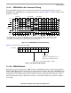

Memory Controller
MPC8260 PowerQUICC II Family Reference Manual, Rev. 2
Freescale Semiconductor 11-51
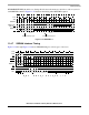
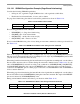
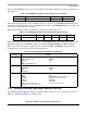
Now, from the SDRAM device point of view, during an ACTIVATE command, its address port should look
like Table 11-27.
Table 11-20. indicates that in order to multiplex A[6–19] over A[15–28] PSDMR[SDAM] must be 001
and, because the internal bank selects are multiplexed over A[15–16] PSDMR[BSMA] must be 010 (only
the lower two bank select lines are used).
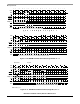
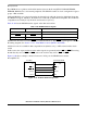
During a
READ/WRITE command, the address port should look like Table 11-28.
Because AP alternates with A[9] of the row lines, set PSDMR[SDA10] = 011. This outputs A[9] on the
SDA10 line during the ACTIVATE command and AP during READ/WRITE and CBR commands.
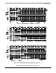
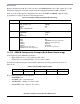
Table 11-29. shows the register configuration. Not shown are PSRT and MPTPR, which should be
programmed according to the device refresh requirements.
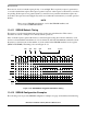
11.5 General-Purpose Chip-Select Machine (GPCM)
Users familiar with the MPC8xx memory controller should read Section 11.5.4, “Differences between
MPC8xx’s GPCM and MPC82xx’s GPCM,” first.
Table 11-27. SDRAM Device Address Port during ACTIVATE Command
“A[0–14]” A[15–16] A[17–28] A[29–31]
— Internal bank select (A[6–7]) Row (A[8–19]) n.c.
Table 11-28. SDRAM Device Address Port during READ/WRITE Command
“A[0–14]” A[15–16] A[17] A[18] A[19] A[20–28] A[29–31]
— Internal bank select Don’t care AP Don’t care Column n.c.
Table 11-29. Register Settings (Bank-Based Interleaving)
Register Settings
BR
x
BA Base address
PS00 = 64-bit port size
DECC00
WP0
MS010 = SDRAM-60x bus
EMEMC0
ATOM00
DR0
V1
OR
x
SDAM1111_1100_0000
LSDAM00000
BPD01
ROWST010
NUMR011
PMSEL0
IBID0
PSDMR PBI0
RFEN1
OP000
SDAM001
BSMA010
SDA10011
RFRC from device data sheet
PRETOACT from device data sheet
ACTTOROWfrom device data sheet
BL0
LDOTOPREfrom device data sheet
WRC from device data sheet
EAMUX0
BUFCMD0
CL from device data sheet