
User manual

Memory Controller
MPC8260 PowerQUICC II Family Reference Manual, Rev. 2
Freescale Semiconductor 11-53
11.5.1 Timing Configuration
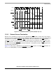
If BRx[MS] selects the GPCM, the attributes for the memory cycle are taken from ORx. These attributes
include the CSNT, ACS[0–1], SCY[0–3], TRLX, EHTR, and SETA fields. Table 11-31 shows signal
behavior and system response.
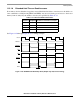
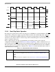
11.5.1.1 Chip-Select Assertion Timing
From 0 to 30 wait states can be programmed for PSDVAL generation. Byte-write enable signals (WE) are
available for each byte written to memory. Also, the output enable signal (OE
) is provided to eliminate
external glue logic. The memory banks selected to work with the GPCM have unique features. On system
reset, a global (boot) chip-select is available that provides a boot ROM chip-select prior to the system
being fully configured. The banks selected to work with the GPCM support an option to output the CS line
at different timings with respect to the external address bus. CS can be output in any of three
configurations:
• Simultaneous with the external address
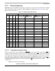
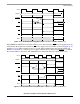
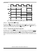
Table 11-31. GPCM Strobe Signal Behavior
Option Register Attributes Signal Behavior
TRLX Access ACS CSNT
Address to CS
Asserted
CS Negated to
Address Change
WE Negated to
Address/Data Invalid
Total Cycles
0Read00 x 0 0 x 2+SCY
1
1
SCY is the number of wait cycles from the option register.
0 Read 10 x 1/4*Clock 0 x 2+SCY
0 Read 11 x 1/2*Clock 0 x 2+SCY
0 Write 00 0 0 0 0 2+SCY
0 Write 10 0 1/4*Clock 0 0 2+SCY
0 Write 11 0 1/2*Clock 0 0 2+SCY
0 Write 00 1 0 0 -1/4*Clock 2+SCY
0 Write 10 1 1/4*Clock -1/4*Clock -1/4*Clock 2+SCY
0 Write 11 1 1/2*Clock -1/4*Clock -1/4*Clock 2+SCY
1Read00 x 0 0 x 2+2*SCY
1 Read 10 x (1+1/4)*Clock 0 x 3+2*SCY
1 Read 11 x (1+1/2)*Clock 0 x 3+2*SCY
1 Write 00 0 0 0 0 2+2*SCY
1 Write 10 0 (1+1/4)*Clock 0 0 3+2*SCY
1 Write 11 0 (1+1/2)*Clock 0 0 3+2*SCY
1 Write 00 1 0 0 -1-1/4*Clock 3+2*SCY
1 Write 10 1 (1+1/4)*Clock -1-1/4*Clock -1-1/4*Clock 4+2*SCY
1 Write 11 1 (1+1/2)*Clock -1-1/4*Clock -1-1/4*Clock 4+2*SCY