
User manual

Memory Controller
MPC8260 PowerQUICC II Family Reference Manual, Rev. 2
Freescale Semiconductor 11-57
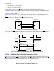
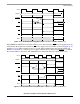
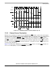
Figure 11-47. GPCM Relaxed-Timing Write (ACS = 1x, SCY = 0, CSNT = 0,TRLX = 1)
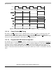
When TRLX and CSNT are set in a write-memory access, the strobe lines, WE[0–7] are negated one clock
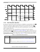
earlier than in the normal case. If ACS ≠ 0, CS is also negated one clock earlier, as shown in Figure 11-48
and Figure 11-49. When a bank is selected to operate with external transfer acknowledge (SETA and
TRLX = 1), the memory controller does not support external devices that provide PSDVAL to complete
the transfer with zero wait states. The minimum access duration in this case is three clock cycles.
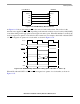
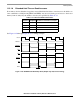
Figure 11-48. GPCM Relaxed-Timing Write (ACS = 10, SCY = 0, CSNT = 1, TRLX = 1)
Clock
Address
PSDVAL
CS
BCTL
x
WE
OE
Data
ACS = 10
ACS = 11
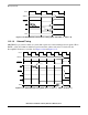
Clock
Address
PSDVAL
CS
BCTL
x
WE
OE
Data
ACS = 10
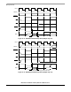
CSNT = 1